- 嘟儿嘟的ScalersTalk第六轮《新概念》朗读持续力训练Day07—20210207
嘟儿嘟_475f
练习材料:L12(1):LifeonadesertislandMostofushaveformedanunrealisticpictureoflifeonadesertisland.Wesometimesimagineadesertislandtobeasortofparadisewherethesunalwaysshines.Lifethereissimpleandgood.Ripefruitf
- 2018-11-17
刘丰成
那啦啦啦啦5饿了let付付付复读额了就看看的了忒天复读佛额特特可怜额就的忒特就看就解雇DHL陪URL去G13会儿铁丝我陪陪着一起儿子二心我头咳嗽DJ邋遢了杰瑞如此怕他邋邋遢遢补补啊吐了咯啦咯啦咯啦咯垃圾咯啦咯啦咯了啦咯啦咯啦咯啦咯啦咯啦咯啦咯啦咯啦咯啦咯啦咯啦咯啦咯啦咯啦咯啦咯啦咯啦咯啦咯啦咯啦咯啦咯啦咯啦咯啦咯啦咯啦咯啦咯啦咯啦咯啦咯了
- 北海的ScalersTalk第六轮新概念朗读持续力训练Day 38 20210207
北海逍遙
练习材料L12(1):Lifeonadesertisland/laɪf//ɒn//ə//ˈdɛzət//ˈaɪlənd/Mostofushaveformedanunrealisticpictureoflifeona/məʊst//ɒv//ʌs//hæv//fɔːmd//ən//ˌʌnrɪəˈlɪstɪk//ˈpɪkʧər//ɒv//laɪf//ɒn//eɪ/desertisland.Wesomet
- IDP规划时间-L12学习总结
学韬
在规划时间的实践过程中,通过时间记录,我找到自己的黄金时间、时间黑洞,并开始刻意的去调整、延长黄金时间,不过期间依然会面对一些惯性上的阻力:比如玩手机超出了时间、遇到事情容易纠结、低效的时间较多、事情太多无法顾及等等。所以接下来,还要对自己的实践继续进阶训练:1、利用工具,增加理性。工具可以帮助提醒,并且辅助思考,让我们从盲目中抽身出来,抬头看路。比如我会用滴答清单记录和整理任务,让自己的行动更有
- IAR Embedded Workbench for Renesas RL78 version 4.21.1
微波家园
软件分享
IAR系统公司最近发布了适用于瑞萨RL78的IAR嵌入式工作台的新版。该版本包括主要的新功能,可简化基于瑞萨低功耗RL78微控制器的应用程序的开发并提高代码质量控制。IAREmbeddedWorkbenchforRenesasRL78版本4.10.1-支持C11语言标准编译器和库增加了对最新C语言标准ISO/IEC9899:2011的支持。注意:新的C库二进制对象接口与该产品的早期版本不兼容。-支
- 瑞萨RL78G12系列单片机使用IAR软件进行仿真设置及与E2接线
ManGo CHEN
工具论与方法论IAR瑞萨单片机E2
目录一、单片机与仿真器连接二、IAR软件在线仿真使用手册一、单片机与仿真器连接E1引脚接线图RL78系列单片机的GND接仿真器的pin2、pin12、pin14RL78系列单片机的VDD接仿真器的pin8RL78系列单片机的Tool0接仿真器的pin5RL78系列单片机的Reset接仿真器的pin10、pin13二、IAR软件在线仿真使用手册1、右击项目工程弹出Options选项进入配置2、配置D
- alios things开发板_AliOS-Things: AliOS Things AliOS家族旗下面向IoT领域的轻量级物联网嵌入式操作系统AliOS Things将致力于搭建云端一体化IoT基...
小仙元
aliosthings开发板
EN|中文AliOSThings发布于2017年杭州云栖大会,是AliOS家族旗下的、面向IoT领域的、高可伸缩的物联网操作系统,于2017年10月20号宣布在github上开源.架构总览AliOSThings支持多种CPU架构,包括:ARM,C-Sky,MIPS,RISCV,rl78,rx600,xtensa等。AliOSThings认证的芯片和模组数量有200+,认证的传感器数量有100+。A
- 《贝肯熊:火星任务》电影票价是多少钱呀?国庆8折买电影票,乐翻天!
桃朵十三
《贝肯熊:火星任务》电影票价是多少钱?官方票价约为36元,特价票仅需19.9元!只需关注微信公众号【奥特快外卖】,并在公众号下方菜单中找到“8折购票”小程序,购买贝肯熊:火星任务的电影票,选择竞价购票,即可享受7-9折的优惠!《贝肯熊:火星任务》看起来将会是一部非常有趣和充满冒险的动画电影。定档海报中的画面非常生动,展示了贝肯熊和机器人G13之间的默契和逗趣,同时也暗示了电影中的神秘和惊险元素。我
- 吸引力6期2阶7隊G13 敏秀
Mika_幸福天使_敏秀
一.照镜子美女,早上好,我爱你么么哒。深深地亲自己一大口,不管眼睛多么睡眼惺忪,不管多么蓬头垢面,不管任何外在因素我深深爱上你了。二.自我嘉许自我嘉许增加自信,自我嘉许增加力量,自我嘉许让我更爱我自己。不管生活遇到多少難關隨時調频1.我嘉许自己做任何决定带上妈妈的角度,这也是从妈妈的角度我才做得出来的决定,我跟哥哥說你儘管處理,孩子我會幫你帶,你別擔心,我想媽媽一定會支持我的決定,兄弟姊妹有難同當
- 第八期-第十天 认识函数
若水9
一、函数的基本用法(一)什么是公式1、是EXCEL工作表中进行数值计算的等式。2、公式输入是以“=”开始的。3、简单的公式有加、减、乘、除等计算。(二)什么是函数1、简而言之,函数就是预先定义好了的公式。比如上例中的公式就可以用函数G13=SUM(G1:G11)代替。2、函数不仅可以简化公式,而且具有仅用运算符连接的一般公式所不能替代的功能。例如查找引用,逻辑判断等等。(三)数组公式输入后按ctr
- 2022-03-14约:38(Z7,L18,G13)
Yiqu
约练分享:今天约练一场,是本周第一场,总38场。在咨询中咨询师很好的陪伴着我,很耐心地听我的生命故事,感谢感谢。整场咨询下来,有一个点,自己在诉说的时候有点哽咽,是说到自己目前在各种人际关系中所感受到的挑战的时候。让自己看到,自己还是很坚强的在一直面对着呢。整场咨询前部分我诉说的比较多,后面是完全跟着咨询师的问题走,在咨询师的带领下走,看到了自己向好的努力和目标,以及自己已经做到的,和自己希望的。
- 2020-04-06-L12
安娜的往事
L12成长日记我们总是发现时间无缘无故的流失,是由于1我们不了解时间,2琐事优先,3.贪心有余而时间不足。我们的生活常常被琐事缠绕,在你想做事的时间却不断的有事情来骚扰,不厌其烦,但是时间却溜走了。有的时间我们想做的事情很多,每一样都想去做,却哪个都没有完成。那么我们的如何高效的处理自己的生活。高效事在正确的时间做正确的事。我们把时间要先做清单记录下来,之后用四个象限来区分:S是重要但不紧急;A是
- 2018-08-29 认识函数
苏静_省思
001基本用法:1.什么是公式:公式79,708=G2+G3+G4+G5+G6+G7+G8+G9+G10+G1101.是EXCEL工作表中进行数值计算的等式。02.公式输入是以“=”开始的。03.简单的公式有加、减、乘、除等计算2.什么是函数:函数93,684=SUM(G2:G11)01.简而言之,函数就是预先定义好了的公式。比如上例中的公式就可以用函数G13=SUM(G1:G11)代替。"02.
- E战到底Day10—认识函数
3队若水
函数是EXCEL表中最重要的部分,也是我最想学习的部分。首先看一下函数与公式的区别:一、基本用法1、公式:1).是EXCEL工作表中进行数值计算的等式。2).公式输入是以“=”开始的。3).简单的公式有加、减、乘、除等计算2、函数:1).简而言之,函数就是预先定义好了的公式。比如上例中的公式就可以用函数G13=SUM(G1:G11)代替。2).函数不仅可以简化公式,而且具有仅用运算符连接的一般公式
- 贝肯熊:火星任务电影票多少钱一张?贝肯熊火星任务什么时候上映?(含特价票)
桃朵十三
今日,喜剧动画电影《贝肯熊:火星任务》宣布定档9月28日国庆档上映。贝肯和新朋友G13接下火星任务,而头顶巨大的兽爪也预示着怪物危机将至,“显眼包特工”贝肯会如何完成这次任务?官方票价在45元左右,特价票低至19.9元一张,您只需要关注微信公众号【奥特快外卖】,并在公众号下方菜单里进入“8折购票”小程序里面购买贝肯熊:火星任务电影票,选择竞价购票,就有7-9折的优惠权限哦!倒霉熊已经推出的两部电影
- IDP成长日志——L12学习心得
蝙蝠侠的披风
利用工具增加理性善用科技产物,如手机/电脑提醒设置、清单/笔记等小工具时间的价值由你定将浪费与闲耗时间转化为投资时间通勤路上听英语不要固化时间,学会灵活调整在时间记录清单里将事件分类重要但不紧急—S级—投资时间重要且紧急—A级—使用时间不重要但紧急—B级—浪费时间不重要不紧急—C级—闲耗时间创造性拖延事情太多无法兼顾时,将不重要的事情尽可能往后拖延
- jieqian的ScalersTalk第四轮新概念朗读持续力训练Day120 20190204
jieqian
#练习材料L12(2):LifeonadesertislandTwomenwhorecentlyspentfivedaysonacoralislandwishedtheyhadstayedtherelonger.TheyweretakingabadlydamagedboatfromtheVirginIslandstoMiamitohaveitrepaired.Duringthejourney,th
- 函数的基本用法
七月与安生_384c
一、基本用法:1.什么是公式①.是EXCEL工作表中进行数值计算的等式。②.公式输入是以“=”开始的。③.简单的公式有加、减、乘、除等计算2.什么是函数"①.简而言之,函数就是预先定义好了的公式。比如上例中的公式就可以用函数G13=SUM(G1:G11)代替。"②.函数不仅可以简化公式,而且具有仅用运算符连接的一般公式所不能替代的功能。例如查找引用,逻辑判断等等。3.数组运算的公式。输入后按ctr
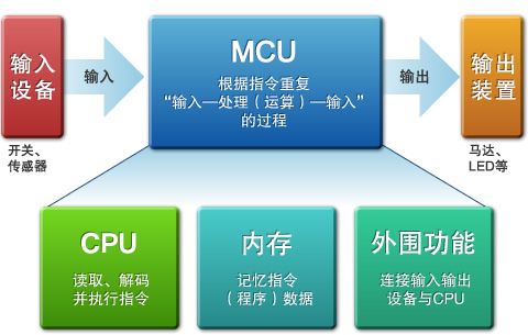
- 低功耗16位MCU:R7F100GLL3CFA、R7F100GLN2DLA、R7F100GLN3CFA、R7F100GLN2DFA是新一代RL78微控制器
Mandy_明佳达电子
明佳达电子单片机嵌入式硬件mcu
产品介绍:RL78/G23低功耗MCU可在41μA/MHzCPU运行频率下工作,功耗低,停止4KBSRAM保持时为210nA。该MCU设有snooze模式排序器,可显著降低间歇工作时的功耗。RL78/G23组具有1.6V至5.5V宽工作电压范围,频率高达32MHz。它们还具有30引脚至128引脚各种封装引脚数和高达768KB闪存。除了增强的模拟和安全特性外,它还在RL78系列中集成了逻辑和事件链路
- 具有超低功耗性能的R7F102GAC3CSP、R7F102GAC2DSP、R7F102G6C3CSP RL78/G22微控制器 16-bit MCU
Summer-明佳达电子
明佳达优势单片机嵌入式硬件mcu
RL78/G22简介:除了具有低电流消耗(CPU工作时:37.5μA/MHz;STOP时:200nA)外,RL78/G22微控制器还配备了丰富的电容触摸通道。完备的16-48引脚封装和32KB-64KB闪存,扩充了新一代RL78通用微控制器的产品线。除了最大工作频率32MHz、广泛的工作电压范围(1.6V-5.5V)和增强的模拟和安全功能之外,SNOOZE模式可编程控制器还可大幅降低间歇工作的功耗
- L12 IDP 规划时间 复盘
野蛮生长_058c
part1:初级训练:时间记录清单分析黄金时间→延长黄金时间→克服惯性阻力。时间规划的开始通过时间记录清单分析出自己的黄金时间。从延长黄金时间开始,这是一项反复和克服惯性拖延的过程,早起和克服拖延一样。我的问题就是心里习惯去满足自己的浪费时间,导致规划的时间被打断。对于我自己而言养成一个好的习惯很重要,当我尝试优先处理重要紧急事件时,我的心里会得到满足,一天都过得比较愉快,当我先去满足自己的浪费时
- 燕玲的Scalers Talk第五轮新概念朗读持续力训练Day109 20200208
少女玲奈酱
练习材料:《新概念英语第三册》Lesson12(2)&13(1)任务配置:L0+L4知识笔记:L0:全文音标——ɛl12(2):laɪfɒnəˈdɛzətˈaɪləndtuːmɛnhuːˈriːsntlispɛntfaɪvdeɪzɒnəˈkɒrəlˈaɪləndwɪʃtðeɪhædsteɪdðeəˈlɒŋgə.ðeɪwɜːˈteɪkɪŋəˈbædliˈdæmɪʤdbəʊtfrɒmðəˈvɜːʤɪn
- 2019-11-13
李然_ca10
E战到底DAY1111.1认识函数-基本用法&11.2进阶用法1.基本用法1.什么是公式1.是EXCEL工作表中进行数值计算的等式。2.公式输入是以“=”开始的。3.简单的公式有加、减、乘、除等计算2.什么是函数1.简而言之,函数就是预先定义好了的公式。比如上例中的公式就可以用函数G13=SUM(G1:G11)代替。2.函数不仅可以简化公式,而且具有仅用运算符连接的一般公式所不能替代的功能。例如查
- 适合家电和消费类应用R7F101GEE4CNP、R7F101GEG4CNP、R7F101GEG3CNP、R7F101GEE3CNP新一代RL78通用微控制器
Mandy_明佳达电子
明佳达电子mcu单片机嵌入式硬件
典型应用•电机控制•电源•照明•一般用途•消费类应用•家用电器•工业自动化•楼宇自动化器件选型1、R7F101GEE4CNP:16BITMCURL78/G2464K40HWQFN-40°C至+125°C2、R7F101GEG4CNP:16BITMCURL78/G24128K40HWQFN-40°C至+125°C3、R7F101GEG3CNP:16BITMCURL78/G24128K40HWQFN-
- 16位 (MCU) R7F101G6G3CSP、R7F101G6E3CSP、R7F101G6G2DSP、R7F101G6E2DSP是新一代RL78通用微控制器
Summer-明佳达电子
明佳达优势单片机嵌入式硬件综合资源
产品描述RL78/G24微控制器具有RL78系列MCU的最高处理性能,CPU工作频率高达48MHz,设有灵活的应用加速器(FAA)。FAA是一款专门用于算法运算的协处理器,可以独立于CPU运行,提供更高处理能力。RL78/G24MCU具有增强的模拟功能和大量定时器,非常适合用于电机控制、电源和照明应用。RL78/G24微控制器还提供丰富的开发环境,包括评估板(快速原型设计板),仅连接USB电缆即可
- Renesas Flash Programmer 下载步骤
weixin_42687361
RENESASFLASHPROGRAMMER下载步骤已有3598次阅读2013-11-216:24第一步:打开RENESASFLASHPROGRAMMER,截图如下:第二步:若有之前打开创建的工程,第二项中会出现这个项目位置,新工程的话选择第一个createnewworkspace,选择basicmode,点击next进入下一步:第三步:选择microcontroller类型,此处选择RL78,过
- 霸道的小米9
xx2586
以前我没用过小米手机,但刷机刷过小米系统,好象那时安卓机流行的是HTC野火(G13),我都忘了是哪一年,只是记得同事对我说过,你怎么不买小米手机呢?为发烧而生,广告好,产品好,但后来他们又说小米系统不稳定容易死机,于是有的转向苹果,有的转向华为荣耀,而我用得最多的是魅族,联想zuk,中兴努比亚,……到后来罗永浩的锤子手机坚果,感觉一两年换一部,到不是喜欢尝鲜,而是安卓机用个一两年,不是电池不行了耗
- 2020-04-15 IDP进阶 L12学习总结
dada大金
来到了进阶营的第二个学习模块了,这个模块更多的是实操的练习内容,目的是通过学习和实操训练来提高我们的执行力。L12的学习内容是通过时间记录清单来分析自己的时间,对时间进行规划以及合理利用,找出自己的黄金时间,延长黄金时间,通过给事件标记分类,来完善时间记录清单并根据自己的使用习惯优化成时间日志。从今天开始,决心要做好每天的时间记录,记录在手机的备忘录上,提高自己的效率。自觉我的黄金时间是在上午,早
- Renesas_iodefine_address
Dawn_Burning
囹圄起舞#Renesas瑞萨嵌入式Renesas瑞萨iodefine.h单片机寻址单片机位操作
RenesasI/O寻址操作写在前面问题发现常见处理追根溯源精益求精写在前面基于RenesasCS+CC编译器中RL78/G13芯片族编程时对未操作时的错误进行追因,思考与总结的小发现和记录。问题发现在瑞萨官方的编译器CS+CC里进行编程中,无法识别我们常用的I/O位操作。例如流水灯实验中,需要频繁的对某个I/O进行位操作赋值来改变他的输出信号,但是编译器只识别整个I/O寄存器。以下用代码段说明:
- L12-规划时间,课程复盘
杰西狗
从认识时间,了解时间,与时间做盆友,认真记录每日的时间清单,这是行动管理的第一步,知己知彼。第二步:规划时间,即在新的每一天开始前,对于全天的梳理和规划。话不多说,先上脑图!L12脑图从脑图中可以看出,本课为实操课程,学习时间记录清单与时间日志。从完成到完美是一个过程,学习时间规划不是一个学了之后就马上能全部消化利用的事儿。从时间清单1.0到2.0的迭代,是一个不断对时间记录优化的过程。先对比一下
- sql统计相同项个数并按名次显示
朱辉辉33
javaoracle
现在有如下这样一个表:
A表
ID Name time
------------------------------
0001 aaa 2006-11-18
0002 ccc 2006-11-18
0003 eee 2006-11-18
0004 aaa 2006-11-18
0005 eee 2006-11-18
0004 aaa 2006-11-18
0002 ccc 20
- Android+Jquery Mobile学习系列-目录
白糖_
JQuery Mobile
最近在研究学习基于Android的移动应用开发,准备给家里人做一个应用程序用用。向公司手机移动团队咨询了下,觉得使用Android的WebView上手最快,因为WebView等于是一个内置浏览器,可以基于html页面开发,不用去学习Android自带的七七八八的控件。然后加上Jquery mobile的样式渲染和事件等,就能非常方便的做动态应用了。
从现在起,往后一段时间,我打算
- 如何给线程池命名
daysinsun
线程池
在系统运行后,在线程快照里总是看到线程池的名字为pool-xx,这样导致很不好定位,怎么给线程池一个有意义的名字呢。参照ThreadPoolExecutor类的ThreadFactory,自己实现ThreadFactory接口,重写newThread方法即可。参考代码如下:
public class Named
- IE 中"HTML Parsing Error:Unable to modify the parent container element before the
周凡杨
html解析errorreadyState
错误: IE 中"HTML Parsing Error:Unable to modify the parent container element before the child element is closed"
现象: 同事之间几个IE 测试情况下,有的报这个错,有的不报。经查询资料后,可归纳以下原因。
- java上传
g21121
java
我们在做web项目中通常会遇到上传文件的情况,用struts等框架的会直接用的自带的标签和组件,今天说的是利用servlet来完成上传。
我们这里利用到commons-fileupload组件,相关jar包可以取apache官网下载:http://commons.apache.org/
下面是servlet的代码:
//定义一个磁盘文件工厂
DiskFileItemFactory fact
- SpringMVC配置学习
510888780
springmvc
spring MVC配置详解
现在主流的Web MVC框架除了Struts这个主力 外,其次就是Spring MVC了,因此这也是作为一名程序员需要掌握的主流框架,框架选择多了,应对多变的需求和业务时,可实行的方案自然就多了。不过要想灵活运用Spring MVC来应对大多数的Web开发,就必须要掌握它的配置及原理。
一、Spring MVC环境搭建:(Spring 2.5.6 + Hi
- spring mvc-jfreeChart 柱图(1)
布衣凌宇
jfreechart
第一步:下载jfreeChart包,注意是jfreeChart文件lib目录下的,jcommon-1.0.23.jar和jfreechart-1.0.19.jar两个包即可;
第二步:配置web.xml;
web.xml代码如下
<servlet>
<servlet-name>jfreechart</servlet-nam
- 我的spring学习笔记13-容器扩展点之PropertyPlaceholderConfigurer
aijuans
Spring3
PropertyPlaceholderConfigurer是个bean工厂后置处理器的实现,也就是BeanFactoryPostProcessor接口的一个实现。关于BeanFactoryPostProcessor和BeanPostProcessor类似。我会在其他地方介绍。PropertyPlaceholderConfigurer可以将上下文(配置文件)中的属性值放在另一个单独的标准java P
- java 线程池使用 Runnable&Callable&Future
antlove
javathreadRunnablecallablefuture
1. 创建线程池
ExecutorService executorService = Executors.newCachedThreadPool();
2. 执行一次线程,调用Runnable接口实现
Future<?> future = executorService.submit(new DefaultRunnable());
System.out.prin
- XML语法元素结构的总结
百合不是茶
xml树结构
1.XML介绍1969年 gml (主要目的是要在不同的机器进行通信的数据规范)1985年 sgml standard generralized markup language1993年 html(www网)1998年 xml extensible markup language
- 改变eclipse编码格式
bijian1013
eclipse编码格式
1.改变整个工作空间的编码格式
改变整个工作空间的编码格式,这样以后新建的文件也是新设置的编码格式。
Eclipse->window->preferences->General->workspace-
- javascript中return的设计缺陷
bijian1013
JavaScriptAngularJS
代码1:
<script>
var gisService = (function(window)
{
return
{
name:function ()
{
alert(1);
}
};
})(this);
gisService.name();
&l
- 【持久化框架MyBatis3八】Spring集成MyBatis3
bit1129
Mybatis3
pom.xml配置
Maven的pom中主要包括:
MyBatis
MyBatis-Spring
Spring
MySQL-Connector-Java
Druid
applicationContext.xml配置
<?xml version="1.0" encoding="UTF-8"?>
&
- java web项目启动时自动加载自定义properties文件
bitray
javaWeb监听器相对路径
创建一个类
public class ContextInitListener implements ServletContextListener
使得该类成为一个监听器。用于监听整个容器生命周期的,主要是初始化和销毁的。
类创建后要在web.xml配置文件中增加一个简单的监听器配置,即刚才我们定义的类。
<listener>
<des
- 用nginx区分文件大小做出不同响应
ronin47
昨晚和前21v的同事聊天,说到我离职后一些技术上的更新。其中有个给某大客户(游戏下载类)的特殊需求设计,因为文件大小差距很大——估计是大版本和补丁的区别——又走的是同一个域名,而squid在响应比较大的文件时,尤其是初次下载的时候,性能比较差,所以拆成两组服务器,squid服务于较小的文件,通过pull方式从peer层获取,nginx服务于较大的文件,通过push方式由peer层分发同步。外部发布
- java-67-扑克牌的顺子.从扑克牌中随机抽5张牌,判断是不是一个顺子,即这5张牌是不是连续的.2-10为数字本身,A为1,J为11,Q为12,K为13,而大
bylijinnan
java
package com.ljn.base;
import java.util.Arrays;
import java.util.Random;
public class ContinuousPoker {
/**
* Q67 扑克牌的顺子 从扑克牌中随机抽5张牌,判断是不是一个顺子,即这5张牌是不是连续的。
* 2-10为数字本身,A为1,J为1
- 翟鸿燊老师语录
ccii
翟鸿燊
一、国学应用智慧TAT之亮剑精神A
1. 角色就是人格
就像你一回家的时候,你一进屋里面,你已经是儿子,是姑娘啦,给老爸老妈倒怀水吧,你还觉得你是老总呢?还拿派呢?就像今天一样,你们往这儿一坐,你们之间是什么,同学,是朋友。
还有下属最忌讳的就是领导向他询问情况的时候,什么我不知道,我不清楚,该你知道的你凭什么不知道
- [光速与宇宙]进行光速飞行的一些问题
comsci
问题
在人类整体进入宇宙时代,即将开展深空宇宙探索之前,我有几个猜想想告诉大家
仅仅是猜想。。。未经官方证实
1:要在宇宙中进行光速飞行,必须首先获得宇宙中的航行通行证,而这个航行通行证并不是我们平常认为的那种带钢印的证书,是什么呢? 下面我来告诉
- oracle undo解析
cwqcwqmax9
oracle
oracle undo解析2012-09-24 09:02:01 我来说两句 作者:虫师收藏 我要投稿
Undo是干嘛用的? &nb
- java中各种集合的详细介绍
dashuaifu
java集合
一,java中各种集合的关系图 Collection 接口的接口 对象的集合 ├ List 子接口 &n
- 卸载windows服务的方法
dcj3sjt126com
windowsservice
卸载Windows服务的方法
在Windows中,有一类程序称为服务,在操作系统内核加载完成后就开始加载。这里程序往往运行在操作系统的底层,因此资源占用比较大、执行效率比较高,比较有代表性的就是杀毒软件。但是一旦因为特殊原因不能正确卸载这些程序了,其加载在Windows内的服务就不容易删除了。即便是删除注册表中的相 应项目,虽然不启动了,但是系统中仍然存在此项服务,只是没有加载而已。如果安装其他
- Warning: The Copy Bundle Resources build phase contains this target's Info.plist
dcj3sjt126com
iosxcode
http://developer.apple.com/iphone/library/qa/qa2009/qa1649.html
Excerpt:
You are getting this warning because you probably added your Info.plist file to your Copy Bundle
- 2014之C++学习笔记(一)
Etwo
C++EtwoEtwoiterator迭代器
已经有很长一段时间没有写博客了,可能大家已经淡忘了Etwo这个人的存在,这一年多以来,本人从事了AS的相关开发工作,但最近一段时间,AS在天朝的没落,相信有很多码农也都清楚,现在的页游基本上达到饱和,手机上的游戏基本被unity3D与cocos占据,AS基本没有容身之处。so。。。最近我并不打算直接转型
- js跨越获取数据问题记录
haifengwuch
jsonpjsonAjax
js的跨越问题,普通的ajax无法获取服务器返回的值。
第一种解决方案,通过getson,后台配合方式,实现。
Java后台代码:
protected void doPost(HttpServletRequest req, HttpServletResponse resp)
throws ServletException, IOException {
String ca
- 蓝色jQuery导航条
ini
JavaScripthtmljqueryWebhtml5
效果体验:http://keleyi.com/keleyi/phtml/jqtexiao/39.htmHTML文件代码:
<!DOCTYPE html>
<html xmlns="http://www.w3.org/1999/xhtml">
<head>
<title>jQuery鼠标悬停上下滑动导航条 - 柯乐义<
- linux部署jdk,tomcat,mysql
kerryg
jdktomcatlinuxmysql
1、安装java环境jdk:
一般系统都会默认自带的JDK,但是不太好用,都会卸载了,然后重新安装。
1.1)、卸载:
(rpm -qa :查询已经安装哪些软件包;
rmp -q 软件包:查询指定包是否已
- DOMContentLoaded VS onload VS onreadystatechange
mutongwu
jqueryjs
1. DOMContentLoaded 在页面html、script、style加载完毕即可触发,无需等待所有资源(image/iframe)加载完毕。(IE9+)
2. onload是最早支持的事件,要求所有资源加载完毕触发。
3. onreadystatechange 开始在IE引入,后来其它浏览器也有一定的实现。涉及以下 document , applet, embed, fra
- sql批量插入数据
qifeifei
批量插入
hi,
自己在做工程的时候,遇到批量插入数据的数据修复场景。我的思路是在插入前准备一个临时表,临时表的整理就看当时的选择条件了,临时表就是要插入的数据集,最后再批量插入到数据库中。
WITH tempT AS (
SELECT
item_id AS combo_id,
item_id,
now() AS create_date
FROM
a
- log4j打印日志文件 如何实现相对路径到 项目工程下
thinkfreer
Weblog4j应用服务器日志
最近为了实现统计一个网站的访问量,记录用户的登录信息,以方便站长实时了解自己网站的访问情况,选择了Apache 的log4j,但是在选择相对路径那块 卡主了,X度了好多方法(其实大多都是一样的内用,还一个字都不差的),都没有能解决问题,无奈搞了2天终于解决了,与大家分享一下
需求:
用户登录该网站时,把用户的登录名,ip,时间。统计到一个txt文档里,以方便其他系统调用此txt。项目名
- linux下mysql-5.6.23.tar.gz安装与配置
笑我痴狂
mysqllinuxunix
1.卸载系统默认的mysql
[root@localhost ~]# rpm -qa | grep mysql
mysql-libs-5.1.66-2.el6_3.x86_64
mysql-devel-5.1.66-2.el6_3.x86_64
mysql-5.1.66-2.el6_3.x86_64
[root@localhost ~]# rpm -e mysql-libs-5.1
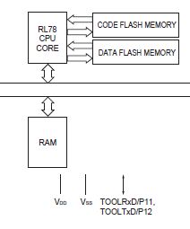
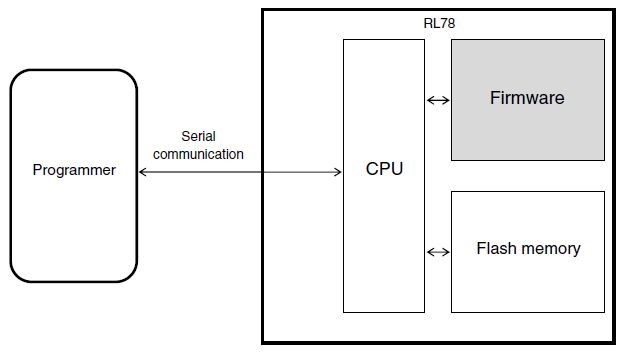 System Outline of Flash Memory Programming in RL78