Here I’m going to demonstrate how to use ModelSim to test out the Virtual JTAG design that I showed in my previous post.
If you’re new to ModelSim with Quartus II, I recommend you look at a post I made awhile back which serves as a quick crash course: Using ModelSim with Quartus II and the DE0-Nano
Quartus II
The first step is to open the Virtual JTAG project we created in the previous post.Here is the top-level schematic:
Adding vJTAG Stimulus
The next step is to setup the stimulus for the Virtual JTAG block which is done by using the vJTAG’s megafunction wizard.First double click the vJTAG block to launch the wizard:
Now keep clicking
Next> until you get to the
General > Stimulation Stimuli tab.
Add in the stimulus as I’ve shown in the image below which is simulating both the Instruction Register (IR), and the Data Register (DR) transmissions:
(See if you can spot the mistake I made in the stimulus. I completely missed it when first setting up this demo but it becomes obvious once we look at the simulation.)Now, if you’re curious like I am and are wondering what/where this stimulus information is stored, navigate and open the vJTAG.v file within the vJTAG.qip in the Project Explorer:
Convert HDL from Schematic
Unfortunately, ModelSim doesn’t allow the top-level to be a schematic file (.bdf), however Quartus has provided us with a handy tool that quickly generates a Verilog file from a schematic.From the menu, use File > Create / Update > Create HDL Design File from Current File...
Since the free version of ModelSim only allows you to simulate with a single HDL language, and not mixed, be sure to select Verilog HDL in the dialog box:
Next, you will need to add this newly created Verilog file to your project, right click on the
Files in the
Project Navigator:
Followed by selecting and adding the file in the subsequent dialog box:
Unfortunately, you’ll also have to remove the
InitialTest.bdf schematic from the project, otherwise Quartus will complain about duplicate declarations of the InitialTest block. (I want to write a nice TCL script that can help automate this dance, but currently we’ll have to do this manually.)
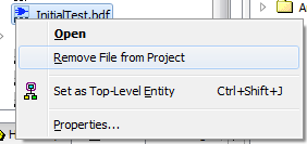
Just right click on the schematic and click remove. (Don’t worry this won’t delete the schematic by default.)
Starting ModelSim
You’ll need to run the Analysis & Synthesis portion of the compilation process to prepare the files for ModelSim:If you get the error: Can’t compile duplicate declarations of entity “InitialTest” into library “work”. Make sure to remove the
InitialTest.bdf schematic from the project.
Using the Tools > Run Simulation Tool > RTL Simulation menu to automatically launch ModelSim and push the design over:
If you get an error at this point, double check to be sure your design is configured to use ModelSim-Altera Version (Setting it to the vanilla version of ModelSim won’t work), also ensure that in the
Tools > Options the path to the ModelSim-Altera is set correctly.
Working with ModelSim
Once ModelSim has started, you should see yourInitialTest project within the
work library
Next, Start the Simulation using the option in the Simulate menu
Set the Design Unit to work.InitialTest
In order to support the vJTAG megafunction block, you’ll need to add the megafunction library to the sim. Add the altera_mf_ver library using the Libraries tab. The _ver suffix selects the verilog version of the library. If you omit this ModelSim will try to use the VHDL version and fail.
After the simulation layout loads, add the signals shown here to the Wave view:
Now advance some simulation time to generate the waveforms:
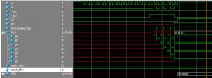
You should see something like the following picture. Looking closely you will see four pulses on the tck signal, corresponding to the stimulus we setup earlier.
Zooming in on the first stimulus event, we see an Instruction Register (IR) shift, switching the ir_in to 1, and thereby asserting the select_DR1 signal
Now zooming in on the second stimulus event, we find the Data Register (DR) shift. We find the tdi signal is captured on the DR1[6:0] register, and once the update data register (udr) signal asserts, the LEDs are updated.
Next, zooming in on the 3rd stimulus event, we find the IR is set back to 0 (setup to be the “bypass” register)
Now finally looking at the last stimulus event, the DR register is updated, but as we alluded to above, I made a mistake in setting up my stimulus. Instead of the DR-Shift being 0×15 the Bit length was set to 1, and as you can see the DR0 is updated to a setting of 1 instead:
Hopefully that was informative. Feel free to leave a comment if you have any questions, or just to let me know if this was helpful to you.


