PCI Express设备驱动 (4,PCIe配置空间和PCI设备中的寄存器)
1、访问PCI配置空间,PCI基本配置空间的读写使用下列函数: 原型定义在
int pci_write_config_byte(struct pci_dev *pdev, int where, u8 *val);
int pci_write_config_word(struct pci_dev *pdev, int where, u8 *val);
int pci_write_config_dword(struct pci_dev *pdev, int where, u8 *val);
向由pdev标识的设备配置空间写入一个、两个或四个字节。
where是偏移量
指针val是要写入的值
2、访问PCI设备的IO或内存空间。
一个PCI设备可实现多达6个IO基地址寄存器,每个寄存器可以是内存地址也可以是IO地址。
PCI配置空间中的6个基地址寄存器,每个都为32位,它们代表PCI的6个IO区域。在linux内核中,PCI设备的IO区域已被集成到通用资源管理,所以要想获得PCI设备的基地址在存储器域的物理地址,要通过下面的函数:
unsigned long pci_resource_start(struct pci_dev *pdev, int bar);
该函数返回6个PCI IO区域中的第bar个的基地址值(存储器域的物理地址)。bar代表基地址寄存器(baseaddress register),取值为0到5.

unsigned long pci_resource_start(struct pci_dev *pdev, int bar);
该函数返回6个PCI IO区域中的第bar个的尾地址值(存储器域的物理地址)。bar代表基地址寄存器(baseaddress register),取值为0到5.
// 将存储器域的物理地址映射为虚拟地址;
// mem = ioremap(phymem, pci_resource_len(pdev, 0));
void *ioremap(unsigned long phys_addr, unsigned long size)
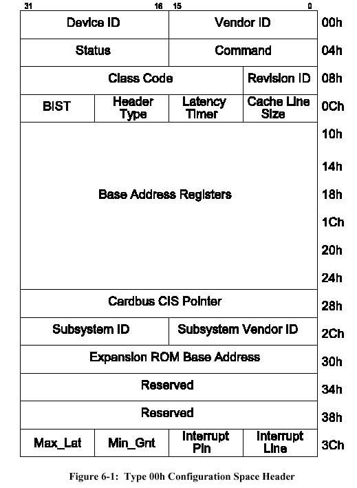
3、PCI基本配置空间
4、PCI设备(Virtex-5 FPGAs)中的寄存器
DMA Control and Status Wrapper
The DMA control and status wrapper is the main block with which the host system processor communicates and the main control for DMA operations. The wrapper is composed of two logical blocks:
• DMA Control/Status Register File
• Internal Control Block
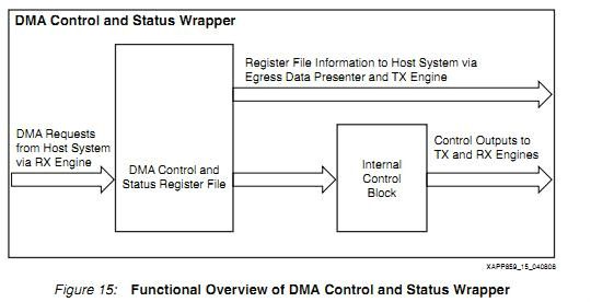
Figure 15 shows the high-level block diagram overview of the wrapper and the connections between the two subblocks.
The logical blocks in this reference design are designed to operate on DMA transfers up to a maximum of 4 KB at a time. This includes the posted packet slicer, non-posted packet slicer, and DMA-to-DDR2 interface blocks. To support transfer sizes larger than 4 KB via the hardware, it is necessary to break up large DMA transfers, i.e., transfers larger than 4 KB, into smaller chunks that the overall hardware design can handle. The DMA Control/Status Register File and Internal Control Block work in conjunction to allow transfer sizes much larger than 4KB.
The DMA Control/Status Register File provides these general functions:
• Provides a memory-mapped interface to the host system in the form of a simple register file interface using one base address register (BAR)
• Accepts read and write DMA transfer requests up to 1 MB in size
• Breaks up DMA transfer requests larger than 4 KB into a sequence of smaller DMA transfers and feeds these small transfers to the Internal Control Block
The Internal Control Block provides these general functions:
• Accepts read and write DMA transfer requests up to 4 KB in size from the
DMA Control/ Status Register File block
• Provides the main control interface to the RX and TX engine blocks
The DMA Control/Status Register File and the Internal Control Block are described in more detail in the following sections.
DMA Control/Status Register File
The DMA Control/Status Register File is memory mapped into the PCI memory space and connected to the user application logic. The host processor accesses the register file through memory read and write cycles on the bus. An Endpoint Block Plus memory base address register facilitates access to the DMA Control/Status Register File.
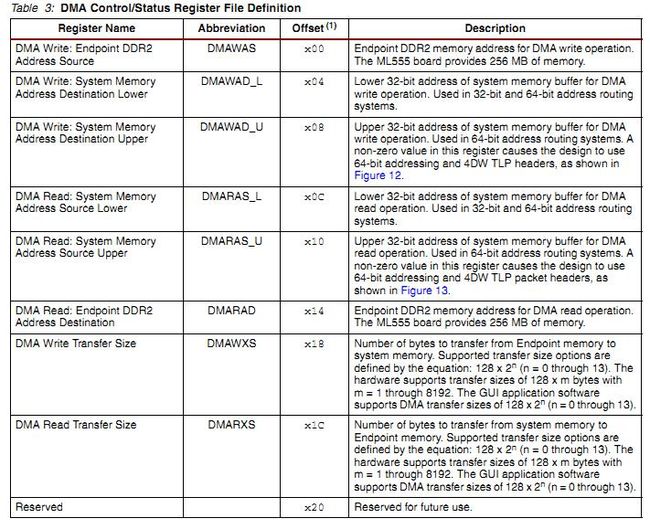
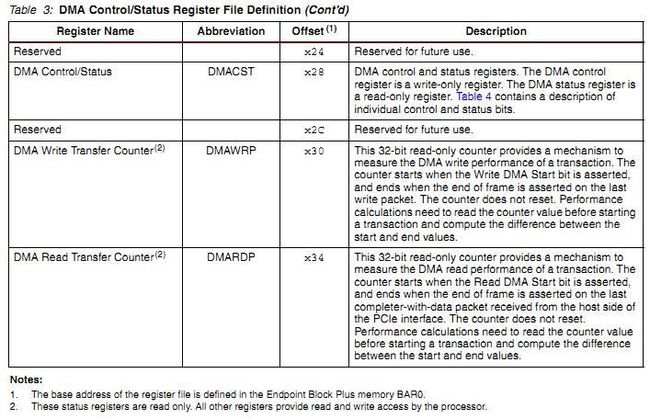
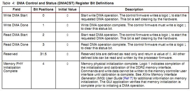
DMA operations are defined in the DMA Control/Status Register File. The processor initiates a DMA transfer by initializing the control registers. DMA completion is provided to the processor through status registers. Table 3 contains a description of the register file. All registers are 32-bit read/write access registers, except as noted.
The read direction denotes ingress to the DDR2 memory. The write direction denotes egress from the Endpoint DDR2 memory. Source and destination addresses must be on 128-byte boundaries. The DMA control and status registers (DMACST) provide control and status of the requested DMA operation as shown in Table 4.
The host PC processor firmware performs these register file accesses to perform a DMA Write operation:
• Verifies that the Write DMA Start bit in DMACST[0] is 0.
• Writes appropriate values to the DMAWAS, DMAWAD_L, DMAWAD_U, and DMAWXS registers for the user-requested DMA transfer specified in the ML555 GUI.
• Writes a 1 to DMACST[0] to initiate the DMA write operation.
• Polls the Write DMA Done bit to determine when the DMA operation is complete.
• Computes the DMA write performance based upon the user-requested transfer size and read-only counter values in the register file. Outputs the result to the GUI log window.
Host PC processor firmware performs these register file accesses to perform a DMA Read operation:
• Verifies that the Read DMA Start bit in DMACST[2] is 0.
• Writes appropriate values to the DMARAS_L, DMARAS_U, DMARAD, and DMARXS registers for the user-requested DMA transfer specified in the ML555 GUI.
• Writes a 1 to DMACST[2] to initiate the DMA read operation.
• Polls the Read DMA Done bit to determine when the DMA operation is complete.
• Computes the DMA read performance based upon the user-requested transfer size and read-only counter values in the register file. Outputs the result to the GUI log window.
Full duplex DMA transfers can be executed by writing a 1 to DMACST[0] and DMACST[2] simultaneously. To keep both transmit and receive channels full, the hardware monitors the state of the channels. For full duplex transfers of 4 KB and under, typically, the hardware executes eight non-posted reads followed by eight posted writes. Full duplex transfers above 4 KB are not executed on any fixed pattern.
Using the host PC processor to poll the register file for status, indicating a DMA read or write completion, can impact the translation layer throughput of this design. After starting a DMA operation, the host PC processor waits for a programmed delay time before polling the endpoint register file to determine if the DMA transfer has completed. The programmed delay time is more than enough time to complete the largest DMA transfer size supported by the design. Polling after the DMA transfer has completed has no impact on the transaction layer throughput of the design.
Several state machines are located in the DMA Control/Status Register File that work in conjunction to feed the Internal Control Block with smaller transfers. These state machines are capable of breaking up a large transfer on the following boundaries: 4 KB, 2 KB, 1 KB, 512 bytes, 256 bytes, and 128 bytes. The state machines break a large transfer request on the largest possible boundaries and transfer a series of smaller requests to the Internal Control Block. For example, a 9600 byte transfer is broken into these smaller transfer sizes:
• 2 x 4 KB
• 1 x 1 KB
• 1 x 256 bytes
• 1 x 128 bytes
The state machines automatically increment the source and destination addresses and transfer size DMA parameters for the smaller sub-transfers and pass these parameters to the Internal Control Block.
