笔试总结(二)
1、控制信号从快时钟域到慢时钟域
与同步器相关的一个问题是来自发送时钟域的信号可能在被慢时钟域采样之前变化。
将慢时钟域的控制信号同步到快时钟域通常不是问题,因为快时钟域将对慢时钟域的控制信号进行一次或多次采样。 在异步时钟域之间传递一个控制信号时,简单的双触发器同步器通常就足够了。
但是如果将控制信号从较快的时钟域传递到较慢的时钟域时,可能会出现问题,来自快时钟域的控制信号必须宽于较慢时钟的周期。否则如下图所示,快时钟域的控制信号无法被采样到慢时钟域。 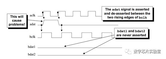
该问题的一个解决方案是扩展快时钟域的控制信号,使得控制信号至少被慢时钟域采样一次。
该问题的第二个解决方案是将快时钟域的控制信号同步到慢时钟域,然后将同步信号通过另一个同步器传回快时钟域作为
acknowledge信号。虽然这种方式是一种非常安全的跨时钟域信号传输方式,但是存在相当大的延迟。
2、使用握手信号在时钟域之间传递数据
可以使用握手控制信号在时钟域之间传递数据。但是在使用握手信号时,控制信号越多,将数据从一个时钟域传递到另一个时钟域的延迟时间越长。
对于许多跨时钟域数据传递,简单的双线握手控制就足够了。发送方将数据放在数据总线上,然后将“data_valid”信号同步到接收时钟域。当新时钟域识别“data_valid”信号的时候,接收方将数据寄存到新时钟域的寄存器中。然后通过同步器向发送方传递“acknowledge”信号。当发送方识别同步后的“acknowledge”信号时,发送方可以改变被驱动到数据总线上的数据。
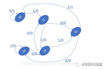
3、一个16bit序列,每个clk左移一位,要求检测5的倍数
方法(1):使用一个状态机实现
s0 : 表示余0
s1 : 表示余1
s2 : 表示余2
s3 : 表示余3
s4 : 表示余4
一开始16bit全为0,所以是s0状态(表示余0),如果下一bit进来1,那就是16’h0001,就是s1状态(余1)。如果下一bit进来0,那就是16’h0002,就是s2状态(余2)。依次类推。只有在s0状态,out输出1。
module five_1(
    input clk,
    input rst_n,
    input a,
    output reg b
);

reg[15:0] seq;

reg a_reg ;
always@ (posedge clk or negedge rst_n) begin
    if (!rst_n)
        a_reg <= 0;
    else
        begin
            a_reg <= a;
        end
end

always@ (posedge clk or negedge rst_n) begin
    if (!rst_n)
        seq <= 16'b0;
    else
        begin
            seq <= {seq[14:0],a_reg};
        end
end

parameterS0 = 3'b000,S1 = 3'b001,S2 = 3'b010,S3 = 3'b011,S4 = 3'b100 ;
reg[2:0] current_state,next_state ;
always@(posedgeclk or negedge rst_n) begin
    if(!rst_n) begin
        current_state <= S0 ;
        b <= 1'b0 ;
    end
    else begin
        current_state <= next_state ;
        if(current_state == S0) begin
            b <= 1 ;
        end
        else begin
            b <= 0 ;
        end
    end
end

always@(*)begin
    case(current_state)
        S0:begin
            if(a == 1'b1) next_state = S1 ;
            else next_state = S0 ;
        end
        S1:begin
            if(a == 1'b1) next_state = S3 ;
            else next_state = S2 ;
        end
        S2:begin
            if(a == 1'b1) next_state = S0 ;
            else next_state = S4 ;
        end
        S3:begin
            if(a == 1'b1) next_state = S2 ;
            else next_state = S1 ;
        end
        S4:begin
            if(a == 1'b1) next_state = S4 ;
            else next_state = S3 ;
        end
    endcase
end


endmodule
方法(2):把这个16bit数看做是4个16进制数
假设该数是ABCD,则这个数字的十进制为A * 16 ^ 3 + B * 16 ^ 2 + C * 16 ^ 1 + D * 16 ^ 0,可以展开为A *(15+1) ^ 3 + B * (15+1) ^ 2 + C * (15+1) ^ 1 + D * (15+1) ^ 0。移除能被5整除的项-----A + B + C + D,所以只需要判断A + B + C + D能否被5整除。
module five_2(
	input clk,
	input rst_n,
	input a,
	output reg b
);

reg [15:0] seq;
always @ (posedge clk or negedge rst_n) begin
	if(!rst_n) begin
		seq <= 16'b0;
	end
	else begin
		seq <= {seq[14:0],a};
	end
end

always @ (posedge clk or negedge rst_n) begin
	if(!rst_n) begin
		b <= 1'b0;
	end
	begin
		b <= (((seq[15:12] + seq[11:8] + seq[7:4] + seq[3:0]) % 5)== 0);
	end
end

endmodule
测试代码:
`timescale 1ns/1ps
module five_tb();
reg clk;
reg rst_n;
reg a;
wire b;


always #1 clk=~clk;

initial
begin
   clk=0;
   rst_n=1;
   a=0;
   #4
   rst_n=0;
   #4
   rst_n=1;
   #2
   a=0;
   #2
   a=1;
   #2
   a=0;
   #2
   a=1;
   #2
   a=0;
   #30
   $stop;
end

five_1 five_inst(
   .clk(clk),
   .rst_n(rst_n),
   .a(a),
   .b(b)
);
endmodule
4、复数计算(a+bj) * (c+dj) = (ac - bd) + (bc + ad)j,,需要四个乘法器才能在一个时钟周期里计算完成,如何优化才能只要三个乘法器在一个时钟周期里计算完成。
思路(1):
ac -bd = (a – b)d + (c – d)a
ad+ bc = (a - b)d + (c + d)b
(a- b)d可以复用
思路(2):
ac-bd =a(c-d)+d(a-b)
bc+ad =c(a+b)-a(c-d)
a(c-d)可以复用
思路(3):bc + ad = (a+b)(c+d) – ac-bd
ac和bd可以复用
思路(4):bc + ad = (a-b)(d-c) +ac+bd
ac和bd可以复用
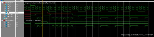
5、时钟输入clk_in,sel为时钟控制信号,sel为0输出clk_in,sel=1,输出clk_in的四分频时钟,要求异步复位,保持时钟的完整性。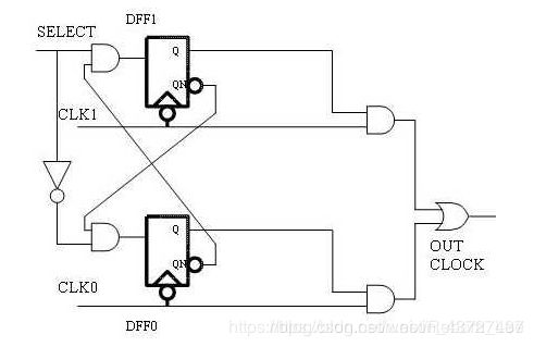
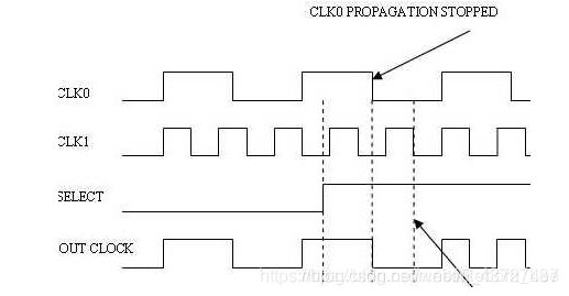
首先SELECT为0,也就是在CLK0的下降沿采样寄存SELECT(取反后)信号与CLK0相与,输出时钟为CLK0;
当在图中时刻SELECT由低电平变为高电平,此时未到CLK0的下降沿,寄存器的输出还将一直是高电平(SELECT之前为0,取反为1),当到达CLK0的下降沿时刻,采样到SELECT为高电平,那么!SELECT为0,也就是上半部分电路从此无效,上半部分电路有效,此时需要等到CLK1的下降沿采样SELECT值,在此之前,输出仍未CLK0,到达CLK1的下降沿后,输出变成了CLK1和SELECT的与,也就是CLK1。由图可见,输出时钟完美切换,并没有出现斩波信号以及毛刺。
module clk_div(
	input clk_in,
	input rst_n,
	output clk_div4
);

reg [1:0] cnt;
always @ (posedge clk_in or negedge rst_n) begin
	if(!rst_n) begin
		cnt <= 2'b0;
	end
	else begin
		cnt <= cnt + 1'b1;
	end
end
assign clk_div4 = cnt[1];

endmodule


module clk_switch(
	input clk_a,
	input clk_b,
	input rst_n,
	input sel,

	output clk_o
);

reg clk_a_en;
reg clk_b_en;

always @ (negedge clk_a or negedge rst_n) begin
	if(!rst_n) begin
		clk_a_en <= 1'b0;
	end
	else begin
		clk_a_en <= ~sel & ~clk_b_en;
	end
end

always @ (negedge clk_b or negedge rst_n) begin
	if(!rst_n) begin
		clk_b_en <= 1'b0;
	end
	else begin
		clk_b_en <= sel & ~clk_a_en;
	end
end

assign clk_o   =   (clk_a & clk_a_en) | (clk_b &clk_b_en) ;
endmodule


module clk_switch_top(
    input clk_in,
    input sel,
    input rst_n,
    output clk_o
);
wire clk_b;
clk_div clk_div_inst(
    .clk_in(clk_in),
    .rst_n(rst_n),
    .clk_div4(clk_b)
);

clk_switch clk_switch_inst(
    .clk_a(clk_in),
    .clk_b(clk_b),
    .rst_n(rst_n),
    .sel(sel),
    .clk_o(clk_o)
);

endmodule

`timescale 1ns/1ps
module clk_switch_tb;

 reg    clk_in   ;
 reg    rst_n   ;
 reg    sel     ;
 wire   clk_o   ;

 always #3 clk_in = ~clk_in;

 initial
 begin
     clk_in = 0;
     sel = 0;
     rst_n = 1;
     #10
     rst_n = 0;
     #7
     rst_n = 1;
     #10
     sel = 1;
     #10
     sel = 0;
     #37
     sel = 1;


 end
clk_switch_top top_inst(
    .clk_in(clk_in),
    .sel(sel),
    .rst_n(rst_n),
    .clk_o(clk_o)
);

endmodule
切换电路如果是上升沿触发,那么会出现毛刺
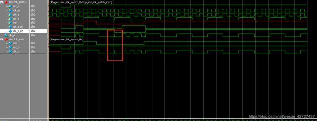
关于造成这种情况的具体原因,我第一个猜测是:两个时钟呈倍数关系,起始上升沿时对齐的。第二个猜测是:上升沿触发,使得clkb_en的高电平和clkb的上升沿是对齐的,所以会出现毛刺。而如果是下降沿触发的话,那么会出现,clka_en或者clkb_en由高变低的时候,接下来有半个时钟周期的低电平所以会完全释放
目前觉得猜测二是最有道理的,具体原因还得查查。
当选择(SELECT)输入稳定的时候(或者为高电平或者为低电平),这两个控制触发器处于相反的状态,两个时钟输入中的一个驱动时钟输出。 当选择(SELECT)输入变化时,这个影响要等到原来的选择的时钟源的下一个下降沿复位它的控制触发器之后才会有。输出时钟信号然后会保持低电平直到新选择时钟的下一个下降沿置位它的控制触发器,使得新选择的时钟来驱动输出时钟。 任何时钟切换都开始于原来选择的时钟变低时,输出时钟然后会保持低电平直到新选择的时钟先变低然后再变高。再也不会出现runt脉冲或输出毛刺。 如果选择(SELECT)输入的时序导致控制触发器进入亚稳态,这并不会有影响,因为输出时钟被输入时钟驱动为低电平(而不管控制触发器的状态
6、如下图所示的一个LFSR结构,初值如图所示,在4个时钟周期之后,寄存器中的值,从左到右的16进制表示?
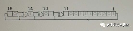
变化前:X[16]、X[15]、X[14] 、X[13] 、X[12]、X[11] 、X[10]、X[9] 、X[8]、X[7]、X[6]、X[5]、X[4]、X[3]、X[2]、X[1]
变化后:X[1] 、X[16]、X[15]^ X[1]、X[14] ^ X[1]、X[13]、X[12] ^ X[1]、X[11]、X[10]、X[9]、X[8]、X[7]、X[6]、X[5]、X[4]、X[3]、X[2]
初值为:10_1_01_10011100001
四个周期之后为:0001_1010_1100_1110
7、设计一个序列信号发生器电路,能在CLK信号作用下周期性输出“0010110111”的序列信号
 module sequence_generator(
      input clk ,
      input rst_n ,
      output out_sequence
  );

  reg [9:0] sequence  ;
  always@(posedge clk or negedge rst_n) begin
      if(!rst_n) begin
          sequence <= 10'b0010110111 ;
      end
      else begin
          sequence <= {sequence[8:0],sequence[9]} ;
      end
  end

  assign out_sequence = sequence[9] ;

  endmodule
8、设计一个自动饮料售卖机,共有两种饮料,其中饮料A每个10分钱,饮料B每个5分钱,硬币有5分和10分两种,并考虑找零。要求用状态机实现,定义状态,画出状态转移图,并用Verilog完整描述该模块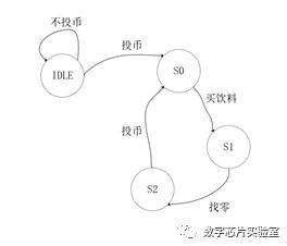 用户必须按照投币-买饮料-找零的顺序依次操作
每轮购买操作中,用户只能投币一次,不然会发生吞币!
投币大小不能比购买饮料的价格小
module machine(
	input clk,
	input rst_n,

	input [2:0] button,   //button[0] --coin_in ;button[1]   --drink_in ;button[2]-- coin_out
	input coin,
	output reg coin_out,
	output reg drink_out
);

parameter IDLE = 2'b00;
parameter S0 = 2'b01;
parameter S1 = 2'b10;
parameter S2 = 2'b11;

reg [1:0] current_state;
reg [1:0] next_state;

always @ (posedge clk or negedge rst_n) begin
	if(!rst_n) begin
		current_state <= IDLE;
	end
	else begin
		current_state <= next_state;
	end
end


always @ (*) begin
	case(current_state)
		IDLE : if(button[0]) begin
					next_state = S0;
			   end
			   else begin
					next_state = IDLE;
			   end
		S0 :  if(button[1]) begin
					next_state = S1;
			  end
		S1 :  if(button[2]) begin
					next_state = S2;
			  end
		S2 :  if(button[0]) begin
					next_state = S0;
			  end
	endcase
end


reg coin_in_reg;
reg drink_in_reg;
always @ (posedge clk or negedge rst_n) begin
	if(!rst_n) begin
		coin_out <= 0;
		drink_out <= 0;
		coin_in_reg <= 0;
		drink_in_reg <= 0;
	end
	else begin
		case(current_state)
			IDLE : begin
						coin_out <= 0 ;
						drink_out <= 0 ;
						drink_in_reg <= 0 ;
						if(button[0]) begin
							coin_in_reg <=  coin_in ;
						end
						else begin
							coin_in_reg <= 0 ;
						end
					end
			S0 : begin
					coin_out <= 0 ;
					drink_out <= 0 ;
					if(button[1]) begin
					    drink_in_reg <= drink_in;
					end
					else begin
					    drink_in_reg <= 0 ;
				    end
				 end
			S1 : begin
					coin_out <= 0 ;
					if(coin_in_reg>= drink_in_reg) drink_out <= drink_in_reg ;
					else                            drink_out <= 1'b0 ;
				 end
			S2 : begin
					drink_out <= 0 ;
					drink_in_reg <= 0 ;
					if(button[0]) begin
					    coin_in_reg <=  coin_in ;
					end
					else begin
					    coin_in_reg <= 0 ;
					end
					if(coin_in_reg> drink_in_reg) coin_out <= 1'b1 ;
					else                           coin_out <= 1'b0 ;
				 end
		endcase
	end
end


endmodule
9、请实现对(1011001)2的序列检测功能,模块每拍并行输入2bit,且输入顺序为高位在先,当检测到序列,输出一拍高脉冲。
相当于检测10–11–00–1x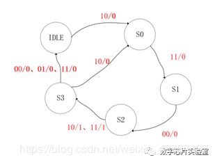
module sequence_checker_2bit(
	input clk,
	input rst_n,
	input [1:0] sequence_in,
	output reg pulse_out
);


parameter IDLE = 3'b000;
parameter S0   = 3'b001;
parameter S1   = 3'b010;
parameter S2   = 3'b011;
parameter S3   = 3'b100;

reg [2:0] current_state;
reg [2:0]    next_state;

always @ (posedge clk or negedge rst_n) begin
	if(!rst_n) begin
		current_state <= IDLE;
	end
	else begin
		current_state <= next_state;
	end
end

always @ (*) begin
	case(current_state)
		IDLE : if(sequence_in==2'b10) begin
					next_state = S0;
			   end
			   else begin
					next_state = IDLE;
			   end
		S0   : if(sequence_in==2'b11) begin
					next_state = S1;
			   end
			   else if(sequence_in==2'b10)begin
					next_state = S0;
			   end
			   else begin
					next_state = IDLE;
			   end
		S1   : if(sequence_in==2'b00) begin
					next_state = S2;
			   end
			   else if(sequence_in==2'b10) begin
					next_state = S0;
			   end else begin
					next_state = IDLE;
			   end
		S2   : if(sequence_in==2'b11 || sequence_in==2'b10) begin
					next_state = S3;
			   end
			   else begin
					next_state = IDLE;
			   end
		S3   : if(sequence_in==2'b10) begin
					next_state = S1;
			   end
			   else begin
					next_state = IDLE;
			   end
	endcase
end

always @ (posedge clk or negedge rst_n) begin
	if(!rst_n) begin
		pulse_out <= 1'b0;
	end
	else if(next_state==S3) begin
		pulse_out <= 1'b1;
	end
	else begin
		pulse_out <= 1'b0;
	end
end

endmodule
10、setup time , hold time含义,说明setup time和hold time会出现负值的原因。
setup time是指在触发器的时钟信号触发之前,数据要求稳定不变的时间。
hold time是指在触发器的时钟信号触发之后,数据需要稳定不变的时间。
在考虑时钟skew的情况下,setup time和hold time需要满足:
T + Tskew > Tsetup + Tco + Tdelay
Thold + Tskew < Tco + Tdelay
由上所知:setup time违例可能是因为工作频率过大,工艺库标准单元速度慢,触发器之间组合逻辑太长
hold time违例能使因为skew 过大,触发器之间组合逻辑太短。
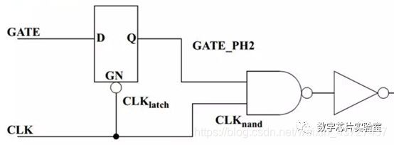
11、请画出一种安全的门控时钟结构?
12、请画出下面verilog代码对应的电路图。
wire [1:0] a;
reg b;
always @ (*)begin
case(a[1:0])
2’b00: b = 1’b0;
2’b01: b = 1’b1;
2’b10: b = 1’b1;
2’b11: b = 1’b0;
endcase
end
化简后:
b = a[1] ^ a[0]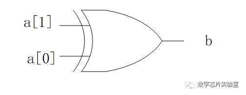
13、画出检测10010序列的状态转移图,并用verilog实现。
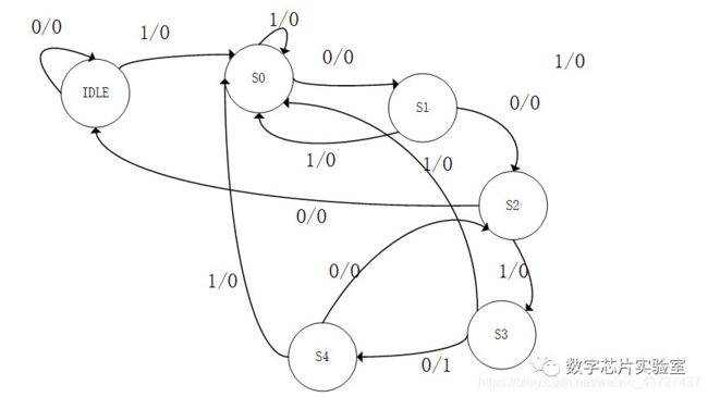
module check(
	input clk,
	input rst_n,
	input data_in,
	output reg data_out
);

parameter IDLE = 3'b000;
parameter S0   = 3'b001;
parameter S1   = 3'b010;
parameter S2   = 3'b011;
parameter S3   = 3'b100;
parameter S4   = 3'b101;

reg [2:0] current_state;
reg [2:0] next_state;

always @ (posedge clk or negedge rst_n) begin
	if(!rst_n) begin
		current_state <= IDLE;
	end
	else begin
		current_state <= next_state;
	end
end

always @ (*) begin
	case(current_state)
		IDLE : if(data_in==1'b1) begin
					next_state = S0;
			   end
			   else begin
					next_state = IDLE;
			   end
		S0   : if(data_in==1'b0) begin
					next_state = S1;
			   end
			   else begin
					next_state = S0;
			   end
		S1   : if(data_in==1'b0) begin
					next_state = S2;
			   end
			   else begin
					next_state = S0;
			   end
		S2   : if(data_in==1'b1) begin
					next_state = S3;
			   end
			   else begin
					next_state = IDLE;
			   end
		S3   : if(data_in==1'b0) begin
					next_state = S4;
			   end
			   else begin
					next_state = S0;
			   end
		S4   : if(data_in==1'b0) begin
					next_state = S2;
			   end
			   else begin
					next_state = S0;
			   end
		default : next_state = IDLE;
	endcase
end

always @ (posedge clk or negedge rst_n) begin
	if(!rst_n) begin
		data_out <= 1'b0;
	end
	else if(next_state==S4) begin
		data_out <= 1'b1;
	end
	else begin
		data_out <= 1'b0;
	end
end

endmodule
14、将一个串行执行的C语言算法转化为单拍完成的并行可综合的verilog
C语言源码如下:
unsigned charcal_table_high_first(unsigned charvalue)
{
    unsigned char i ;
unsigned  char checksum = value ;
    for (i=8;i>0;--i)
    {
        if (check_sum& 0x80)
        {
            check_sum = (check_sum<<1) ^ 0x31;
        }
        else
        {
            check_sum = (check_sum << 1);
        }
    }
    return check_sum;
}
#include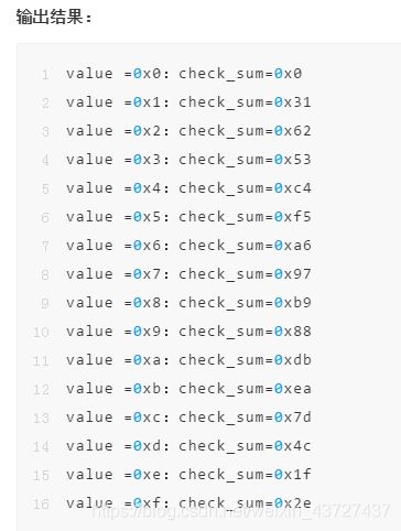
该算法的逻辑如下:
输入一个8bit的数,首先判断最高位是否为1,如果为1则左移一位,并且和8‘b00110001异或;如果最高位不为1则左移一位。此过程执行8次。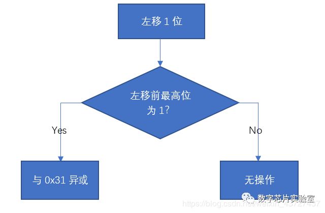
任何数与0异或都等于他本身,即0 ^ x = x,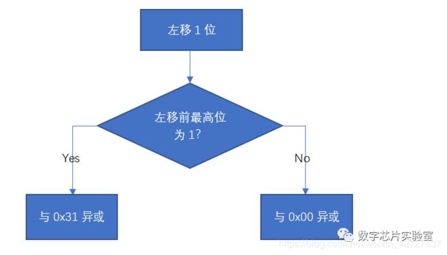
8’h31 = 8’b00110001, 8’h00 = 8’b00000000,设左移前最高位为M,可以将判断左移前最高位是否为1的过程省略,直接与8’b00MM000M异或,此时流程图可以简化为:
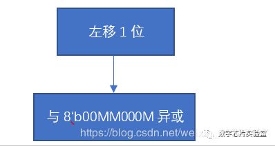
由此,我们可以将循环解开,设输入为一个8bit数C[7:0],下面为解循环过程。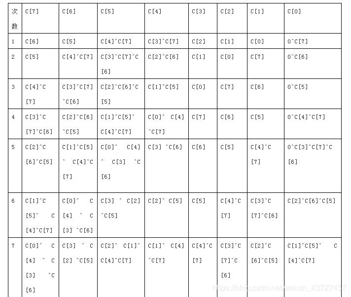
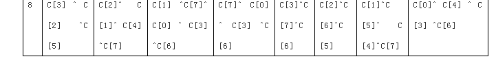
综上所述,verilog代码实现如下:
module loop1(
   input clk,
   input rst_n,
   input [7:0] check_sum,
   output reg [7:0] check_sum_o
);
//reg [7:0] check_sum_o;
always @ (posedge clk or negedge rst_n)
       if(!rst_n)
              begin
                     check_sum_o<= 8'h0;
              end
       else
              begin
                     check_sum_o[7]<= check_sum[3]^check_sum[2]^check_sum[5];
                     check_sum_o[6]<= check_sum[2]^check_sum[1]^check_sum[4]^check_sum[7];
                     check_sum_o[5]<= check_sum[1]^check_sum[7]^check_sum[0]^check_sum[3]^check_sum[6];
                     check_sum_o[4]<= check_sum[7]^check_sum[0]^check_sum[3]^check_sum[6];
                     check_sum_o[3]<= check_sum[3]^check_sum[7]^check_sum[6];
                     check_sum_o[2]<= check_sum[2]^check_sum[6]^check_sum[5];
                     check_sum_o[1]<= check_sum[1]^check_sum[5]^check_sum[4]^check_sum[7];
                     check_sum_o[0]<= check_sum[0]^check_sum[4]^check_sum[3]^check_sum[6];
              end

endmodule
module loop2(
   input clk,
   input rst_n,
   input [7:0] check_sum,
   output  reg [7:0] check_sum_o
);
integer i;
//reg [7:0] check_sum_o;
reg [7:0] ccc;
always @ (posedge clk or negedge rst_n)
       if(!rst_n) begin
            check_sum_o<= 8'h0;
       end
       else begin
			ccc <= check_sum;
            for(i=0;i<8;i=i+1)
            begin
                ccc ={ccc[6:0],1'b0}^({8{ccc[7]}} & 8'h31);
            end
			check_sum_o <= ccc;
          end

endmodule
封装C语言成函数
module loop3(
   input clk,
   input rst_n,
   input [7:0] check_sum,
   output  reg [7:0] check_sum_o

);

integer i;

function [7:0] cal_table_high_first;
       input[7:0] value;
       reg[7:0] ccc ;
       reg[7:0] flag ;
       begin
           ccc= value;
           for(i=0;i<8;i=i+1)
               begin
               flag= ccc & 8'h80 ;
               if(flag!= 0) ccc = (ccc <<1) ^ 8'h31 ;
               else ccc = (ccc <<1)  ;
               end
           cal_table_high_first= ccc;
       end

endfunction

always @ (posedge clk or negedge rst_n)
       if(!rst_n)
              begin
                     check_sum_o<= 8'h0;
              end
       else
              begin
                    check_sum_o<= cal_table_high_first(check_sum) ;
              end

endmodule
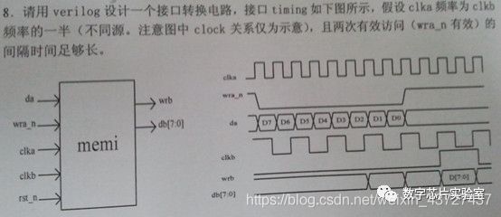
module interface_change(
	input clka,
	input wra_n,
	input da,

	input clkb,
	output [7:0] db,
	output wrb
);


reg [7:0] data;
always @ (posedge clka) begin
	if(!wra_n) begin
		data <= {data[6:0],da};
	end
end

reg wra_n_reg1;
reg wra_n_reg2;

always @ (posedge clkb) begin
	wra_n_reg1 <= wra_n;
	wra_n_reg2 <= wra_n_reg1;
end

wire wra_n_check ;
assign wra_n_check = wra_n_reg1&&(!wra_n_reg2) ;
assign wrb = wra_n_check ;
assign db = (wra_n_check == 1'b1) ? data :0 ;

endmodule


endmodule
16、如图所示时序路径示意图,椭圆表示组合逻辑,FF1/FF2表示寄存器,A表示数据输入端口,CLK表示时钟输入端口,Z表示数据输出端口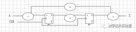
A. 只要在端口CLK上创建时钟,即可约束A->Z之间的组合逻辑的延时
B. 只要在端口Z上设置输出延时,即可约束FF2 -> Z之间的组合逻辑的延时
C. 只要在端口CLK上创建时钟,即可约束FF1->FF2之间的组合逻辑的延时
D. 只要在端口A上设置输入延时,即可约束A->FF1之间的组合逻辑的延时
解释:
在逻辑综合时,一般有4中path group:
Input to reg :输入端口到寄存器,通过set_input_delay设置输入端口外的延时,来约束组合逻辑延时
Tclk – T1 – Tinput_delay – Tsetup > 0
Reg to reg :寄存器到寄存器,通过create_clock,约束为时钟周期
Tclk - Tcq - T2 - Tsetup> 0;
Reg to output :
我们设置 Tclk和Toutput_delay,从.lib/.db库里面读入Tcq,工具就会约束优化T3组合逻辑
Tclk - Tcq - T3 - Toutput_delay > 0;
Input to output;
我们设置Tinput_delay + Toutput_delay,工具就会约束优化T3组合逻辑
Tclk - Tinput_delay -T3 - Tout_delay > 0;
也可以直接设置 set_max_delay
17、中断是处理器能完成并行性,实时操作的一种重要手段,请选出如下有关中断的正确描述?
A:以上表述都不对
B:中断的响应过程中,保护程序计数器的作用是cpu能找到中断处理程序的入口地址,
C:cpu在响应中断期间,原来的程序依然可以执行
D:中断响应中,断点保护,现场保护由用户编程完成。
B:保护程序计数器的作用是cpu退出中断,找到主程序的入口地址。
C:原程序是中止的,不能运行
D:现场保护由系统自动(编译器)完成
18、以下关于FPGA和ASIC描述正确的是:
A:FPGA开发周相对短
B:相同工艺下,ASIC能跑更快的时钟
C:FPGA更注重面积的要求。
D:ASIC批量生产时成本相对低
ABD