基于android7.1+msm8937读取ADC采样值
基于android7.1+msm8937读取ADC采样值
读取给设备供电的电压,比如16V,通过监控ADC(Analog-to-Digital Conversion)值来知道电源波动情况和实际给设备供电的电压。
1. 硬件电路设计
输入的VCC_16V_IN经过R206和R207分压连接到MPP1_16V_ADC也就是PMI8937_MPP1


ADCs are directly controlled by the PMIfuel gauge
2. 硬件原理
2.1 MPP1路由到SPMI
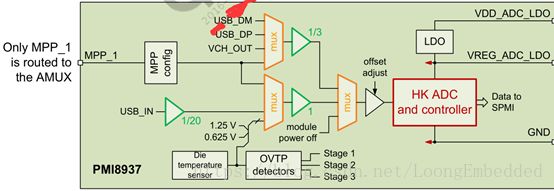
Analog input – inputs are routed to the analog multiplexer switch network; if selected, andthat analog voltage is routed to the HK/XO ADC for digitization(数字化).

2.2 PMI8937模拟输入通道
PMI8937模拟多路复用器和扫描功能,见下图

ADC电压值=(16*100*1024)/((1024+100)*1024)=1.4234875V。
此图来之于《80-P2561-1_PMI8937 POWER MANAGEMENTIC DEVICE SPECIFICATION》文档。有两个MPP_1,选择哪个通道呢?因为计算出来到MPP1的最大电压是1.4V<1.5V,所以选择16通道(十进制),相当于十六进制的0x10,确定为16通道后,scaling也确定为1了。
2.3 ADC性能参数

16-bit dedicatedcurrent ADC (15 bits plus sign bit) ,16位的采样分辨率。
2.4 MPP1配置为ADC的参考示例
驱动电压值的驱动可以参考kernel\msm-3.18\Documentation\devicetree\bindings\hwmon\qpnp-adc-voltage.txt
-------------------------------非常重要----------------------------------
Client device example:
/* Add to the clients node that needs theVADC channel A/D */
client_node {
qcom,client-vadc= <&pm8941_vadc>;
};
/* Clients have an option of measuring ananalog signal through an MPP.
MPP block is not part of the VADC block but is an individual PMIC
block that has an option to support clients to configure an MPP as
ananalog input which can be routed through one of the VADC pre-mux
inputs. Here is an example of how to configure an MPP as an analog
input */
/* Configure MPP4 as an Analog input toAMUX8 and read from channel 0x23 */
/* MPP DT configuration in the platform DTfile*/
mpp@a300{ /* MPP 4 */
qcom,mode= <4>; /* AIN input */
qcom,invert= <1>; /* Enable MPP */
qcom,ain-route= <3>; /* AMUX 8 */
qcom,master-en= <1>;
qcom,src-sel= <0>; /* Function constant */
};
/* VADC Channel configuration */
chan@23{
label= "mpp4_div3";
reg= <0x23>;
qcom,decimation= <0>;
qcom,pre-div-channel-scaling= <1>;
qcom,calibration-type= "absolute";
qcom,scale-function= <0>;
qcom,hw-settle-time= <0>;
qcom,fast-avg-setup= <0>;
};
3. 软件实现
3.1 相关的驱动、设备树和内核文档
(1) ADC驱动
Kernel/msm-3.18/drivers/hwmon/qpnp-adc-common.c
Kernel/msm-3.18/drivers/hwmon/qpnp-adc-voltage.c
qpnp-adc-voltage.c
Qualcomm's QPNP PMIC Voltage ADC Arbiter
QPNP PMIC Voltage ADC (VADC) providesinterface to clients to read
Voltage. A 15 bit ADC is used for Voltagemeasurements. There are multiple
peripherals to the VADC and the scope ofthe driver is to provide interface
for the USR peripheral of the VADC.
Kernel/msm-3.18/hwmon/qpnp-adc-current.c
(2) ADC DTS
Kernel/msm-3.18/arch/arm/boot/dts/qcom/msm-pmi8937.dtsi
Kernel/msm-3.18/arch/arm/boot/dts/qcom/msm-pm8937.dtsi
(3) ADC DTSI文档
Kernel/msm-3.18/Documentation/devicetree/bindings/hwmon/qpnp-adc-voltage.txt
Kernel/msm-3.18/Documentation/devicetree/bindings/hwmon/qpnp-adc-current.txt
4. 软件实现
4.1 设备树
Y:\trunk\kernel\msm-3.18\arch\arm\boot\dts\qcom\msm-pmi8937.dtsi
(1) 配置MPP1为模拟输入
pmi8937_mpps: mpps {
spmi-dev-container;
compatible= "qcom,qpnp-pin";
gpio-controller;
#gpio-cells= <2>;
#address-cells= <1>;
#size-cells= <1>;
label= "pmi8937-mpp";
mpp@a000{
reg= <0xa000 0x100>;
qcom,pin-num= <1>;
qcom,mode= <4>; // AIN input ,QPNP_PIN_MODE_AIN
qcom,invert= <1>; // Enable MPP,QPNP_PIN_INVERT_ENABLE
qcom,ain-route= <0>; //AMUX 5,QPNP_PIN_AIN_AMUX_CH5,AMUX 8----3 ????
qcom,master-en= <1>;//Enable features within the pin block based on configurations.(GPIO/MPP)
qcom,src-sel= <0>; //Function constant
//status= "disabled";
};
重点说明下qcom,ain-route = <0>;
- qcom,ain-route: Set the destination for analog input.
QPNP_PIN_AIN_AMUX_CH5 = 0, (MPP)
QPNP_PIN_AIN_AMUX_CH6 = 1, (MPP)
QPNP_PIN_AIN_AMUX_CH7 = 2, (MPP)
QPNP_PIN_AIN_AMUX_CH8 = 3, (MPP)
QPNP_PIN_AIN_AMUX_ABUS1= 4, (MPP)
QPNP_PIN_AIN_AMUX_ABUS2= 5, (MPP)
QPNP_PIN_AIN_AMUX_ABUS3= 6, (MPP)
QPNP_PIN_AIN_AMUX_ABUS4= 7 (MPP)
从kernel\msm-3.18\arch\arm\boot\dts\qcom\msm-pm8937.dtsi下面的信息
mpp@a300 {
/*MPP4 - CASE_THERM config */
reg= <0xa300 0x100>;
qcom,pin-num= <4>;
qcom,mode= <4>; /* AIN input */
qcom,invert= <1>; /* Enable MPP */
qcom,ain-route= <3>; /* AMUX 8 */
qcom,master-en= <1>;
qcom,src-sel= <0>; /* Function constant */
status= "disabled";
};
知道MPP4是采用AMUX8,推断为MPP1采用AMUX5,所以配置为qcom,ain-route= <0>;如果配置为AMUX8,经测试获取到的值不正常,而且波动很大。
(2) 配置通道16
根据上面的计算,输入到MPP1的电压<1.5V,所以选择16通道,下面增加通道相关的
//kandi add for 0x10 channel
chan@10{
label= "power16v_detect";
reg= <0x10>;
qcom,decimation= <0>;// 0 : 512, Sampling rate to use for the individual channelmeasurement.
qcom,pre-div-channel-scaling= <0>;//0 : {1, 1},Pre-div used for the channel before the signal isbeing measured
qcom,calibration-type= "ratiometric";//Reference voltage to use for channel calibration.
qcom,scale-function= <0>;//0 : Default scaling to convert raw adc code to voltage.
qcom,hw-settle-time= <0>;//Settling period for the channel before ADC read.
qcom,fast-avg-setup= <0>;//0 : 1,Average number of samples to be used for measurement
};
(3)
pmi8937_vadc: vadc@3100 {
compatible= "qcom,qpnp-vadc";
reg= <0x3100 0x100>;
…
4.2 Lk阶段读取电压值
bootable\bootloader\lk\dev\pmic\pm8x41\include\pm_vadc_hc.h
/* API: Set the PM8x41 MPP pin as ADC */
void pm8x41_enable_mpp_as_adc(uint16_tmpp_num);
没有验证过。
Qcom LK阶段如何使用ADC介绍
https://blog.csdn.net/loongembedded/article/details/80577667
4.3 ADB读取电压值
adb root
adb shell
cat/sys/bus/spmi/devices/qpnp-vadc-15/power_in_detect
![]()
4.4 内核上读取adb数值
(1) 获取ADC设备
pdata->id_vadc_dev =qpnp_get_vadc(&(pdata ->dev), "ltp_tem");
(2) 读取电压值
rc = qpnp_vadc_read(data->id_vadc_dev,P_MUX4_1_1, &results); //0x13=19=P_MUX4_1_1
相关的API接口和结构体

示例代码

参考:
VADC获取温度值
https://blog.csdn.net/u012719256/article/details/79296034