【开源电机驱动】H 桥驱动-软件篇
原文地址:http://www.modularcircuits.com/blog/articles/h-bridge-secrets/h-bridge-control/
本文为作者翻译校正稿件,含个人理解批注
H-bridge Control
H 桥驱动方式-硬件篇
Introduction
引言
In the previous part of the series we went through the various circuits that can take logic level digital signals and make them suitable for driving the gates of the bridge power FETs. These circuits range from trivial to complex, and have some interesting properties, like turn-on and –off delay or limits on duty cycle that will have implications for our current discussion.
在本系列的前几部分,我们通过各种可以改变逻辑电平的数字信号电路,来驱动桥式功率场效应管的栅极。这些电路从简单到复杂,它们都具有一些有趣的性质,如开通关断延迟或占空比的限制,这将影响我们当前的讨论。
In this article we will step further back from the ‘bare metal’ of the H-bridge and concentrate on the digital control of the bridge. The discussion will concentrate on how to generate the various control signals and how to implement the different drive modes we’ve discussed before.
在本文中,我们将进一步远离H桥的纯物理部分,专注于H桥的数字控制。 集中讨论怎么生成各种控制信号以及如何实现我们之前讨论的不同驱动模式。
For the most part, the detailed implementation of the driver and the bridge itself (PMOS or NMOS devices, etc.) are not a concern here, though occasionally we’ll have to take the special requirements of those parts of the design into consideration.
在大多数情况下,栅极驱动和H桥本身(PMOS 或 NMOS 设备等)的详细实现在这里并不需要考虑,尽管有时我们必须考虑设计中这些部分的特殊要求。
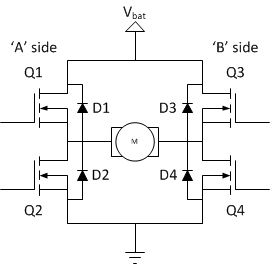
I will use the following h-bridge element notations during the article:
在本文中,我将使用以下H桥模型(双N沟道MOSFET):
Bridge driver control
H桥驱动控制
As we’ve seen before there are many drivers and there are many ways those drivers need to be controlled as well. For both low- and high-side drivers, the two basic schemes are active low or active high control.
如前文所言,会有许多栅极驱动,并且还有许多方法控制这些栅极驱动。 对于低侧和高侧驱动而言,低电平有效控制或高电平有效两种基本的控制方案。
In active low control, the FET is closed, when the control signal is low, or 0:
在低电平有效控制中,当控制信号为低电平或0时,FET闭合(导通):
| control 控制 | FET state 场效应晶体管状态 |
| 0 | close (conduct) “闭合” “导通” |
| 1 | open (doesn’t conduct) “开路” “不导通” |
In active high control, the sates are the opposite:
在高电平有效控制中,情况正好相反:
| control 控制 | FET state 场效应晶体管状态 |
| 0 | open (doesn’t conduct) “开路” “不导通” |
| 1 | close (conduct) “闭合” “导通” |
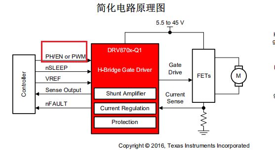
With half-bridge drivers, which control one low and one high-side FET, the options are more complicated. Some simply expose two control signals (active low or high) each for the two controlled transistors. Some however have an ‘enable’ and a ‘PWM’ pin for example. Again, these can be active low or active high. I will not bore you with all the possible combination (check the datasheet for your part for the exact details) but one example could be the following:
对于控制一个低端和一个高端FET的半桥驱动器,选择更加复杂。 有些芯片只留两个控制脚(低电平有效或高电平有效)。
此外,有些芯片(应该是全桥芯片)具有“使能”和“ PWM输入”引脚。 同样,它们可以是低电平有效或者高电平有效。 我将不会列出所有可能的组合(你可以查看他们的数据手册获得这些信息),下面是一个示例:
Another control method is when the driver exposes only a single, three-state control input. When driven low, or high, one or the other FET conducts, when left floating, the both FETs are open:
另一种控制方法是当驱动程序仅公开单个三态控制输入时。 当被驱动为低电平或高电平时,一个或另一个FET导通,当悬空时,两个FET均断开(今天的H桥或者半桥驱动已经很成熟,一般而言,厂家会在设计芯片时加入下拉电阻,以避免出现悬浮状态):
| control | High-side state | Low-side state |
| 0 | open (doesn’t conduct) | close (conduct) |
| 1 | close (conduct) | open (doesn’t conduct) |
| Z | open (doesn’t conduct) | open (doesn’t conduct) |
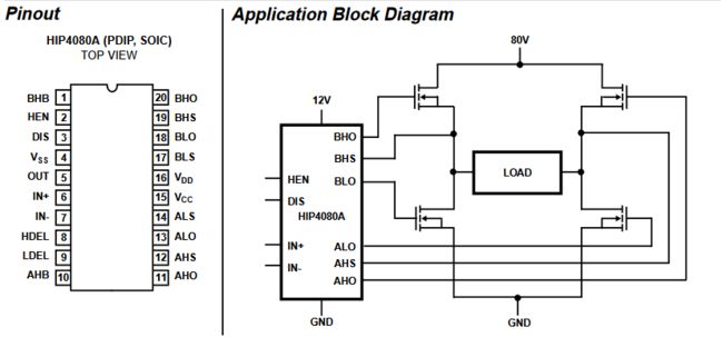
Full-bridge drivers can expose an even wider variety of control options, since they drive four FETs. Sometimes they have four control signals for each individual FETs, or would look like two independent half-bridge circuits. Other times, they combine the control signals for the ‘A’ side and ‘B’ side of the bridge into fewer control signals. When that happens (like the HIP4080A from Intersil), the driver might start to limit the control patterns and drive modes you can use the bridge with. If you recall, both the ‘A’ and the ‘B’ side have three possible states, so a full-bridge can have six possible (static) states. This needs a minimum of 3 digital control signals, so if a full-bridge driver exposes less, you should expect limitations. Yet others (the HIP4080A is a good example for that as well) combine some analog functions to help implement closed-loop control.
全桥驱动器可以驱动四个FET,因此它们提供了更多的控制选项。 有时它们为每个单独的FET提供四个控制信号,或者看起来像两个独立的半桥电路。 有时,它们会将电桥“ A”侧和“ B”侧的控制信号合并为较少的控制信号。 这种情况下(例如Intersil的HIP4080A),驱动程序可能会开始限制H桥可以使用的控制模式和驱动模式。 回忆一下,“ A”侧和“ B”侧都有三种可能的状态,因此全桥可以有六个可能的(静态)状态。 这至少需要3个数字控制信号,因此,如果全桥驱动方式较少较少,应该是有一些限制。 某些驱动器(HIP4080A也是一个很好的例子)结合了一些模拟功能来帮助实现闭环控制。(这款芯片大概是1995年的了,已经跟不上发展的脚步了,今天的全桥驱动基本是傻瓜式的,自带了保护,方便易用)
You can find the exact control method for your chosen driver in its datasheet.
您可以在数据表中找到所选驱动程序的精确控制方法。
To simplify the discussion in the following chapter, I will assume that the bridge driver has four independent, active-high input signals, one for each FET. If your driver needs a different type of control, you can easily convert the signals to your particular needs.
为了简化下一章的讨论,我们假设H桥的驱动信号有四个,高电平有效,每个 FET 一个。如果你的驱动方式与此不同,你可以很容易地转换到你需要的信号。
Basic drive-mode mapping
基本驱动模式映射
Let’s first examine, what control states each of the inputs need for the various drive-modes.
让我们首先了解,对于各种驱动模式,每个输入需要什么控制状态。
Let’s start with the lock anti-phase drive in the forward direction:
让我们从锁定反相驱动方式的正向导通开始:
| Lock anti-phase drive, FWD | On-time | Off-time |
| Q1_CTRL 1 ctrl | 1 | 0 |
| Q2_CTRL 2 ctrl | 0 | 1 |
| Q3_CTRL 3 ctrl | 0 | 1 |
| Q4_CTRL 4 ctrl | 1 | 0 |
For sign-magnitude drive in the forward direction, using high-side off-time conduction we get:
对于正向的符号-幅值驱动,使用高侧对“停机”时的电流进行传导,我们得到:
| Sign-magnitude drive, FWD, high-side | On-time | Off-time |
| Q1_CTRL 1 ctrl | 1 | 1 |
| Q2_CTRL 2 ctrl | 0 | 0 |
| Q3_CTRL 3 ctrl | 0 | 1 |
| Q4_CTRL 4 ctrl | 1 | 0 |
The same sign-magnitude drive in the reverse direction:
同样地,符号-幅值驱动器反向运行时:
| Sign-magnitude drive, REV, high-side | On-time | Off-time |
| Q1_CTRL 1 ctrl | 0 | 1 |
| Q2_CTRL 2 ctrl | 1 | 0 |
| Q3_CTRL 3 ctrl | 1 | 1 |
| Q4_CTRL 4 ctrl | 0 | 0 |
Notice so far how the two ‘a’-side control signals (Q1 and Q2) are always inverse of one another. Same is true for the two ‘b’-side drive signals. One would think that we could simply drive them from the same input, through a simple inverter. Unfortunately in practice that would almost always be a bad idea but we will have to come back to that a bit later.
到目前为止,两个 A 侧控制信号(Q1和 Q2)总是相反的。两个 B 侧的驱动信号也是如此。有人会认为,我们可以使用相同的输入,通过一个简单的反相器来驱动它。不幸的是,在实践中,这不是好主意,我们稍后再来讨论这一点。
For now, let’s finish up the mapping tables for the asynchronous sign-magnitude drive. Here I’ll assume high-side off-time conduction as well. For the forward direction we can use the following table:
现在,让我们完成异步符号幅值驱动方式的映射表。在这里,我也假设电流通过高侧的“非运行状态”时间传导。对于正方向,我们可以使用下表:
| Async. Sign-magnitude drive, FWD, high-side | On-time | Off-time |
| Q1_CTRL 1 ctrl | 1 | 1 |
| Q2_CTRL 2 ctrl | 0 | 0 |
| Q3_CTRL 3 ctrl | 0 | 0 |
| Q4_CTRL 4 ctrl | 1 | 0 |
For the reverse direction:
反向的映射如下:
| Async. Sign-magnitude drive, REV, high-side | On-time | Off-time |
| Q1_CTRL 1 ctrl | 0 | 0 |
| Q2_CTRL 2 ctrl | 1 | 0 |
| Q3_CTRL 3 ctrl | 1 | 1 |
| Q4_CTRL 4 ctrl | 0 | 0 |
There are some other possible drive patterns that would result in one of these three drive modes. We will see if they are useful in a bit, for now let’s just consider these five mappings. By carefully looking at the tables you can see some nice patterns emerge:
还有一些其他可能的驱动模式,最终都会回到这三种驱动模式之一。我们来看看它们是否有用,现在让我们考虑一下这五个映射。通过仔细观察这些表格,你可以看到一些规律:
- For lock anti-phase drive the ‘a’-side control is a mirror image of the ‘b’-side one. The PWM signal should be connected to both sides, but in reverse polarity. 对于锁定反相驱动方式,“ a”侧控制信号是“ b”侧的镜像。PWM 信号应该连接到两侧,但反向(互补).
- For the phase magnitude drive, two FETs are controlled with a constant signal, only one side is driven with the PWM signal. You can change driving direction by swapping which side gets the PWM drive and which one gets the static signals. 对于相位幅值驱动方式,采用恒定信号控制两个场效应管,PWM 信号只驱动一侧。你可以通过交换哪一边得到 PWM 驱动,哪一边得到静态信号来改变驱动方向
- For asynchronous sign-magnitude drive, only one of the four FETs is switching the other three are at constant voltages. The drive direction is changed by deciding which FET to toggle. 对于异步符号幅值驱动器(使用高侧泄放电流),四个场效应晶体管中只有一个进行切换,其余三个为恒定电压。驱动方向通过决定切换哪个 FET 来改变
Power-down state
停电状态
Almost every bridge design needs to have a disabled, or power-down state. There are two possibilities to achieve that. One option is to have at least one of the motor terminals floating. The other is to short the motor terminals together.
几乎每一个H桥设计都需要有一个禁用状态,或关闭电源状态。有两种方法可以实现这一目标。一种方法是使至少一个电动机终端浮空。另一种方法是将电动机的接线端子短路。
For sign-magnitude and asynchronous sign-magnitude drive, this’s simple as at 0% duty-cycle that is exactly what happens. For lock anti-phase drive however a new state needs to be introduced for this purpose. Of the many possibilities, let’s choose the one where both motor terminals are floating for this discussion:
对于符号幅度和异步符号幅度驱动器,这很简单,因为在0% 的占空比工作状态时就会发生这种情况。然而,对于锁定反相驱动器,需要为此引入一个新的状态。在众多的可能性中,让我们选择一个电机终端都浮空的部分进行讨论:
| Lock anti-phase drive | Power-down state |
| Q1_CTRL 1 ctrl | 0 |
| Q2_CTRL 2 ctrl | 0 |
| Q3_CTRL 3 ctrl | 0 |
| Q4_CTRL 4 ctrl | 0 |
In many cases, especially when a microcontroller is in charge of generating the signals for the MOSFETs, it is important that the default power-up state of the bridge is the power-down one. This way, the firmware running on the microcontroller is in no rush of initializing the bridge control signals. It can work on getting the whole system up and running and only after all setup and initialization is done it needs to move the bridge out of power-down into the operational state.
在许多情况下,特别是当微控制器负责为 mosfet 产生控制信号时,电桥的默认启动状态是关闭的是很重要的。这样,运行在微控制器上的固件就不会急于初始化H桥控制信号。它可以让整个系统启动和运行,只有在所有的设置和初始化完成后,才需把H桥从断电状态转换到运行状态。
Many microcontrollers start up with their pins in a high-impedance state, when they can’t source nor sink current. If those pins are connected to the bridge driver inputs, as long as the firmware doesn’t initialize the pins for any other state, the output voltage is not well defined and the wire is susceptible to noise. This can lead to the bridge turning on or worse, getting into a shoot-through condition during startup. To prevent this from happening, its good practice to include pull-up or pull-down resistors on each bridge control pin to make sure they are at a well-defined voltage at all times. The value of the resistors usually isn’t critical as long as the don’t load the output stages inside the microcontroller too much. It is also good practice to set the resistors up such that they keep the bridge in its power-down state.
许多微控制器启动时,它们的管脚会处于高阻抗状态,这时它们既不能提供电流,也不能吸收电流。如果这些引脚连接到H桥驱动器的输入端,只要固件没有将管脚定位为任何状态,输出电压就是不确定的,而导线容易受到噪声影响。这可能导致H桥开启,或者产生更糟的情况,在启动过程中进入直通状态。为了防止这种情况发生,比较好的的做法是在每个H桥控制引脚上安装上拉或下拉电阻器,以确保它们在任何时候电压是确定的。只要不在微控制器的引脚上添加过多负载,电阻器的值不重要。这也是一个很好的做法,放置电阻,使H桥保持在断电状态。
Shoot-through protection
击穿保护
We’ve mentioned shoot-through several times already in previous parts of the series. We’ve said at the very beginning that the high-side and the low-side switches of an H-bridge on the same side should never ever be turned on at the same time. If that happened, you would create a very low resistance path between your power supply and ground. There are several outcomes of such an experiment and none of them are pleasant. At best, you have some sort of short-circuit protection that trips and your circuit simply looses power. If not, a lot of current will start flowing through your circuit. This current will start heating things up and eventually something will break. It will heat up the battery (because of its internal resistance) and overheated batteries can explode. It will heat up the wires which can melt their plastic insulation. It will heat up the PCB traces, making them de-laminate or even vaporize and destroy the board. It will heat up your FETs and can destroy them as well. You don’t want any of these, so you don’t want shoot-through. Avoiding static shoot-through is fairly simple: just make sure you never close both ‘a’ or ‘b’-side FETs at the same time.
在本系列的前几部分中,我们已经多次提到“击穿”这个词。我们在一开始就说过,同一侧 H 桥的高端和低端开关永远不该在同一时刻打开。如果发生这种情况,电源将会回路。这样的做有几种后果,但没有一个是令人愉快的。也许,你具有短路保护并且这种情况下它会跳闸,但电源因此关断。如果没有短路保护,大量的电流将会通过你的电路。电流会使元器件升温,最终导致它们损坏。它还会加热电池(因为电池有等效内阻),电池过热可能导致爆炸。同时它会加热导线,使电线的塑料绝缘材料熔化。它也会加热 PCB 的铜线,使他们从环氧树脂板上脱离。它会加热你的场效应管,并直接摧毁它们。你并不希望看到这些结果,你要避免它们。避免静态击穿很简单: 确保我们不在同一时刻导通两个“ a”侧或“ b”侧的上下两个场效应管。
The bigger problem is dynamic shoot-through: when you turn one FET off, while turning the other FET on, for a short while both the low and high-side FETs are potentially conducting to a certain degree, creating a – relatively – low resistance path for the supply to flow to ground. This results in a current-spike that – while not as destructive as static shoot-through – is still quite problematic. To prevent this, you have to delay the turn-on of the low-side FET by at least as much as the turn-off time of the high-side FET. The same goes of course for the other transition, when you switch from low-side to the high-side.This technique has many names, dead-time, shoot-through protection, no-overlap PWM, but whatever you call it, unless you know the turn-off times, you can’t time this delay properly. This is one of the reasons I’ve sent so much time in the previous installment talking about turn-on and –off-times and how to calculate and control them.
更棘手的问题是动态击穿:当关闭一个FET时,迅速打开另一个FET,低端和高端FET都可能在一定程度上导通(由于开通和关断的延迟,通常时间很短,由于Q = UIt,因此动态击穿并不像静态击穿那样具有毁灭性),从而产生了一个低电阻电流回路,使得电源通过这个回路到达GND。 这会导致电流尖峰,尽管不像静态击穿那样具有破坏性,但仍然存在很多问题(电流尖峰可能破坏MOSFET,也有可能影响其他器件)。 为避免这种情况,您必须将低侧FET的开启延迟一段时间,这个延迟的时间至少是高侧FET的关闭延迟的时间。 从低端切换到高端时当然也是如此。这种技术具有很多名称,死区时间,击穿保护,无重叠PWM,但无论如何称呼它,必须知道MOSFET的关断时间,否则就无法正确设置此延迟时间。 这是我在上一期中花了很多时间讨论“导通阶段”和“关断阶段”时间以及如何计算和控制该时间的原因之一。
When you do employ shoot-through protection however, you will end up with a different problem: now, instead of having both the low- and high-side FETs conducting for a short while during the transition, you have none of them conduct for a split-second. At the same time – as we’ve discussed several times already – the motor current cannot just stop flowing instantly, so some circuit – the catch diodes – will have to take over. As the diodes usually have a higher loss than the switches themselves, during this short time the heat dissipation of the bridge will be higher than normal. This additional dynamic loss on the bridge gets worse as your shoot-through protection window gets a larger and larger portion of the cycle time. So for really high-frequency operations, tight shoot-through protection window control is needed to minimize this source of heat dissipation. In those applications various dynamic shoot-through protection techniques are becoming more and more popular, mostly as part of the bridge driver circuitry.
然而,当你使用了“直通保护”时,你将面临一个不同的问题:现在,在过渡期间,低边和高边的fet不会同时导通,一瞬间内没有一个fet导通。同时,正如我们已经讨论了好几次的那样,电机电流不能立即停止流动,因此一些电路——寄生二极管——将不得不接管这些电流。由于二极管通常比开关本身具有更高的损耗,因此在这段短时间内,电桥的散热量将高于正常值。这个额外的动态损失在桥上变得越来越严重,因为你的“直通保护”的窗口时间越来越大。因此,在高频操作中,需要严格的“直通保护”窗口时间控制,以尽量减少这种热量产生。在这些应用中,各种动态“直通保护”技术正变得越来越流行,它已成为H桥驱动器电路的一部分。
In many cases, integrated bridge drivers have built-in shoot-through protection circuits with fixed or programmable block-out windows. With those you only have to make sure that your turn-off times are compatible with what the parts can support.
通常情况下,集成的H桥驱动器都有内置的固定或可编程的屏蔽窗口的死区保护电路。有了这些,你只需要确保你的关闭时间是器件支持的。
If you are using a part without such protection or are building your own driver, you’ll have to make sure that proper shoot-through protection is implemented either in HW or in SW.
如果您使用的部件没有这样的死区保护或正在建立自己的驱动程序,你必须通过软件或者硬件的方式确保有适当的死区保护。
Many modern microcontroller PWM implementations give you the option to use two pins that output versions of a single PWM signal, with a programmable no-overlap zone between them, like the SAM7S series from Atmel:
许多现代微控制器的 PWM 模式会给你一个选择,它可以输出一对互补的PWM,它们之间有一个可编程的不重叠区域,就像来自 Atmel 的 SAM7S 系列和当下流行的STM32系列:
External shoot-through protection circuits
外部死区保护电路(硬件)
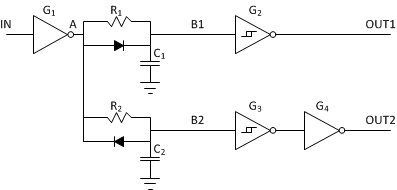
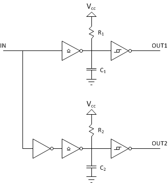
If you need to generate the above wave-forms externally, you can do that for example with the following circuit:
如果你需要在外部产生上述波形,你可以通过下面的电路来实现:
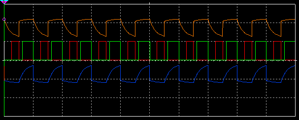
我在Multisim中对以上电路进行了仿真 ,原理图和仿真结果如下:
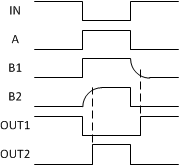
It uses the the R/C circuits to delay the edges of the two outputs, and the diodes to make sure only one of the two edges get delayed. The Schmitt-trigger inverters are needed to clearly define the point where the output switches due to the slow changing of the output of the R/C circuit. The timing diagram of the circuit is the following:
它使用 R/C 电路来延迟两个输出端的边沿,使用二极管来确保只有一个边缘被延迟。由于 R/C 电路输出变化缓慢,需要施密特触发逆变器来清楚地定义输出开关的位置。电路的时序图如下:
You can see how this circuit reproduces the same non-overlapping outputs that we’ve seen at the end of the previous chapter. The delay of the falling edge of OUT1 can be calculated as the following:
你可以看到这个电路是如何重现我们在前一章末尾看到的相同的非重叠输出的。OUT1下降边缘的延迟时间可计算如下:
tdout1 = –R1*C1 ln(Vtl/Voh)
where Voh is the high-level output voltage of the input gate, and Vtl is the low-level trigger voltage of the Schmitt-trigger. Similarly, the delay of the rising edge of OUT2 is the following:
其中 Voh 是输入栅极的高电平输出电压,Vtl 是施密特触发器的反向阈值电压电压。同样,OUT2上升边缘的延迟如下:
tdout2 = –R2C2 ln(1-Vth/Voh)
where Vth is the high-level trigger voltage of the Schmitt-trigger.
其中 Vth 是施密特触发器的正向阈值电压。
With many Schmitt-trigger circuits having their lower and higher threshold voltages set at 1/3 and 2/3 way between 0 and Voh, both time delays end up roughly R1 C1 and R2 C2 respectively.
由于许多施密特触发电路的阈值电压分别设置在0和 Voh 之间的1/3和2/3,所以这两种延时时间近似为 R1C1和 R2C2。
The input gate (G1) can in many cases be the output driver of the PWM output pin, especially in CMOS logic. Many bridge drivers have Schmitt-trigger input stages so if the input polarity works out the right way, the output buffers (G2, G3 and G4) can be eliminated as well. Even if not, a 6-gate Schmitt-trigger chip, like one of the many ariants of the 7414 chip provides a single-chip solution (obviously the normal inverters can also be Schmitt-triggers, they just don’t have to be).
在许多情况下,输入门(G1)可以作为 PWM 输出引脚的输出驱动器,特别是在 CMOS 逻辑中。许多桥驱动器芯片都有施密特触发输入级,因此如果输入极性正确工作,输出缓冲器(G2,G3和 G4)也可以去掉。即使不是这样,一个6通道的施密特触发芯片,就像7414芯片的众多变种之一,也提供了一个单芯片的解决方案(很明显,普通的逆变器也可以是施密特触发器,它们只是没有必要这样做)。
Finally, this circuit doesn’t produce clear high logic levels at B1 and low logic-levels at B2 due to the forward voltage drop of the diodes. Because of that, a relatively high supply voltage needs to be used, otherwise the signal might not clear both tripping-points of the Schmitt-triggers during their edges. With very low supply voltages, a similar, but different technique using open-drain drivers or discrete FETs can be used to create the asymmetrical delays on the rising and falling edges:
最后,由于二极管具有正向压降,该电路在B1处没有产生清晰的逻辑“高”电平,在B2处没有产生明显的逻辑“低”电平。因此,需要使用相对较高的电源电压,否则信号可能无法清除施密特触发器的两个跳闸点。在极低的电源电压下,开漏驱动器或分立场效应晶体管的类似但不同的技术可在上升和下降沿产生不对称延迟:
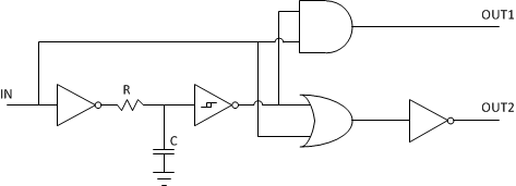
There are many other techniques as well, depending on what type of resources you have available. For example, this one uses a single R/C timing element to generate both types of delays:
还有许多其他技术,这取决于您拥有的资源类型。例如,它使用一个 R/C 延时电路来产生两种类型的延迟:
PWM routing
PWM路径
Let’s re-examine the control patterns in the previous chapter! You’ve seen that some of the four drive signals are constant during the cycles, some are switching. We can use a simplified notation to describe the various modes. Let’s call an external signal PWM, which is 1 during the on-time and 0 during the off-time. Another signal, !PWM does the opposite. Let’s not forget that these signals aren’t exactly inverted versions of one another due to the previously mentioned shoot-through protection requirement. Let’s also create a signal, DIR, which is ‘1’ for forward direction, and ‘0’ for reverse. It’s opposite is !DIR. Note that when changing direction, the same no-overlap change should be observed on this signal pair as well, so \DIR isn’t simply an inverted version of DIR either. With this notation, the drive modes are as follows:
让我们重新看一下前一章中的控制模式!显而易见,四个驱动信号在一个周期内是不变的,其中一些是周期信号(PWM),一些是是开关信号(0和1)。让我们使用简化符号来描述各种驱动模式。对于外部信号 PWM,1表示开通阶段,0表示关断阶段。另一个信号,!PWM 则与它相反。让我们不要忘记,这些信号不完全相反的另一个版本(具有死区时间),由于前面提到的“击穿保护”要求。让我们创建另外一个信号,DIR,1表示正向,0表示反向。与此相反的是 !DIR。注意,当改变方向时,在这个信号对上也应该观察到相同的无重叠的变化,因此 !DIR 也不仅仅是 DIR 的一个翻转版本。有了这个符号,驱动器模式如下:
| Lock anti-phase drive 锁定-反向驱动模式 |
signal 对应符号 |
| Q1_CTRL | PWM |
| Q2_CTRL | !PWM |
| Q3_CTRL | !PWM |
| Q4_CTRL | PWM |
| Sign-magnitude drive 符号-幅值驱动模式 |
low-side off-time current 使用低侧导通关断电流 |
high-side off-time current 使用高侧导通关断电流 |
| Q1_CTRL | PWM | DIR |
| Q2_CTRL | !PWM | !DIR |
| Q3_CTRL | !DIR | !PWM |
| Q4_CTRL | DIR | PWM |
| Asynchronous 异步符号-幅值驱动模式 |
forward, low-side off-time current 正转 低侧导通关断电流
|
forward, high-side off-time current 正转 高侧导通关断电流 |
reverse, low-side off-time current 反转 低侧导通关断电流 |
reverse, high-side off-time current 反转 低侧导通关断电流 |
| Q1_CTRL | PWM | DIR | DIR | DIR |
| Q2_CTRL | !DIR | !DIR | !DIR | PWM |
| Q3_CTRL | !DIR | !DIR | PWM | !DIR |
| Q4_CTRL | DIR | PWM | !DIR | !DIR |
You can see that depending on the drive mode, the control signal routing can be fixed or need to depend on the off-time current conduction path chosen (which can be a design-time decision). In the case of asynchronous sign-magnitude drive, the signal routing needs to be dynamic as even a drive direction change changes the PWM signal routing.
您可以看到,根据驱动模式,控制信号的途径可以是固定的,或者需要依赖于所选择的“非工作时间”电流的传导路径(这可以是一个设计时决策)。在异步符号-幅度驱动模式下,信号的路径需要是动态的,即驱动方向的变化改变了 PWM 信号的路径。
This may or may not be problematic, many microcontrollers have flexible enough I/O pins that make all of the modes possible without external logic. However in many cases the support of asynchronous sign-magnitude drive requires four PWM generators inside the microcontroller, as it might not be possible to get a single PWM source appearing on multiple, configurable pins.
这并不是什么问题,许多微控制器有足够灵活的 I/O 管脚,使所有的模式在没有外部逻辑的情况下成为可能。然而,在许多情况下,支持异步符号幅度驱动的单片机内部需要有四个 PWM 发生器,因为它不可能通过一个单一的PWM源实现输出多个可配置的PWM(STM32的PWM,一般使用一个PWM源,多个通道可以独立控制)。
Another interesting observation is that asynchronous sign-magnitude drive doesn’t use the \PWM signal. As a consequence it doesn’t depend on proper shoot-through protection window setting on the PWM output, so if your microcontroller doesn’t support no-overlap PWM signals and your FET driver doesn’t support shoot-through protection either, this drive mode might still be available to you.
另一个有趣的观察是,异步符号幅度驱动器不使用 !PWM 信号。因此,它不依赖于正确的直通保护窗口设置的 PWM 输出,所以如果你的微控制器不支持带死区的 PWM 信号以及你的 FET 驱动器不支持直通保护,这种驱动模式可能仍然可用。
Complex cycles and heat spreading
复杂的周期和散热
On each of the four FETs (and their catch-diodes) there are two types of loss that generate heat:
四个场效应晶体管(和它们的寄生二极管)上,下列两种类型的损耗将会产生热量:
- Static loss, which is simply I^2Rdson times their conduction percentage per cycle for FETs, and VfI times percentage their conduction percentage per cycle for the catch diodes.
- 静态损耗,简单地说就是I^2*Rdson,即每个周期内的场效应晶体管的损耗,以及寄生二极管,在每个周期的导通时间乘以它的正向压降
- Dynamic loss, which is more complex to calculate but is related to how often the device is turned on or off and how much it spends in between the ‘on’ and ‘off’ states. Dynamic loss on the catch diodes is related to the size of the shoot-through protection window and the actual turn-on and –off times of the FETs.
- 动态损耗,计算起来比较复杂,但与设备的开关频率以及开关状态的损耗有关。寄生二极管的动态损耗与击穿保护窗口的大小和 fet 的实际开关次数有关
The average static loss between the four devices only depends on the drive mode and the duty cycle. The average dynamic loss depends on the switching frequency, the turn-on and –off times and the shoot-through protection window size. Depending on the drive mode however, the generated heat doesn’t get distributed evenly across the four FETs and diodes.
四个设备之间的平均静态损耗仅取决于驱动模式和占空比。平均动态损耗取决于开关频率、开关次数和死区保护窗口大小。然而,根据驱动模式的不同,产生的热量不会均匀地分布在四个场效应晶体管和寄生二极管上。
We’ve seen that in the various drive modes, a different number of FETs are switched:
我们已经看到在不同的驱动模式下,不同数量的 fet 被切换:
- For lock anti-phase drive, all four FETs are switching
- 对于锁定-反相驱动,四个场效应管切换
- For sign-magnitude drive, two FETs are switching
- 对于符号-幅值驱动器,两个场效应管正在切换
- For asynchronous sign-magnitude drive only a single FET is switching
- 对于异步符号-幅值驱动器,只有一个 FET切换
This means that in sign-magnitude drive, the switching FETs will have more dynamic loss (heat) than the non-switching ones. Taking static losses into consideration as well, it’s easy to see that for example in our previous forward driving case Q3 and Q4 together will dissipate more heat than Q1.
这意味着在符号幅度驱动下,开关场效应管比未开关的场效应管有更多的动态损耗(热量)。考虑到静态损失,很容易看到,例如在我们先前的驱动情况下,Q3和Qu4一起将散发比Q1更多的热量。
For asynchronous sign-magnitude drive, the asymmetry is even more obvious: in that case (same forward drive example) Q3 never opens, yet conducts current during the off-time through it’s body-diode. As losses on such a diode are normally higher than on the FET itself, it dissipates even more heat than in the previous case.
对于异步符号-幅值驱动器,不对称性更加明显: 在这种情况下(使用正向驱动的例子) Q3永远不会打开,但在关闭时间通过它的寄生二极管导通。由于二极管的损耗通常比 FET 本身的损耗更高,因此它相比于之前的情况,将会消耗更多的热量。
Finally, for both types of sign-magnitude drive, there’s one FET that never conducts at all.
最后,对于这两种类型的符号-福州驱动器,有一个 FET 从来没有导通。
These imbalances complicate thermal design of the bridge. It would be best if we could spread the heat more evenly across the four devices. We can do that of course mechanically, by mounting them on the same heat-sink, but there are electrical ways to make situation more balanced as well.
这些不平衡使H桥的热设计变得复杂化。如果我们能把热量均匀地分布在这四个设备上最好。当然,可以使用机械元件来做到这一点:把它们安装在同一个散热器上。但是也有一些电子方法可以使热量情况更加平衡。
Lock anti-phase drive
锁定反相驱动
We’ve just discussed that in lock anti-phase drive all four FETs are turned on and off in every cycle. The motor current is conducted through FETs for both the on- and off-time as well. This means that we can’t really optimize the heat-spreading in this mode: dynamic losses are equally distributed already, and static losses depend only on the conduction time of the switches, which depends on the duty cycle (d). Still, let’s examine the behavior of the bridge in this mode so we have something to compare the other options to.
我们刚才讨论了,在锁定-反相驱动器所有四个场效应管是打开和关闭在每个周期。电机电流是通过场效应管进行开关时间以及。这意味着我们不能真正优化在这种模式下的散热: 动态损耗已经是均匀分布的,静态损耗只取决于开关的传导时间,这取决于占空比(d)。不过,让我们检查一下这种模式下桥接器的行为,这样我们就可以对其他选项进行比较。
In lock anti-phase drive the conduction times as a percentage of the cycle time are the following:
在锁相反相驱动器中,传导时间占周期时间的百分比如下:
| Q1 | d/2 |
| Q2 | 100%-d/2 |
| Q3 | 100%-d/2 |
| Q4 | d/2 |
This is pretty much as good as it gets, with the (static) heat dissipation distributed equally among all transistors in the idle state (note that for this drive mode 50% duty cycle corresponds to idle). The further we get from the idle position the more imbalance we have between the FETs.
这是相当好的(静态)热耗散平均分布在所有晶体管的空闲时间(注意,对于这种驱动模式,50%的占空比对应于空闲时间)。离空闲位置(50%)越远,fet之间的不平衡就越大。
For dynamic losses, we’ll just have to repeat the switching table and take a look at it again:
对于动态损失,我们只需要再看一遍表格:
| Lock anti-phase drive, FWD | On-time | Off-time |
| Q1_CTRL 1 ctrl | 1 | 0 |
| Q2_CTRL 2 ctrl | 0 | 1 |
| Q3_CTRL 3 ctrl | 0 | 1 |
| Q4_CTRL 4 ctrl | 1 | 0 |
You see that – as we’ve said before – all four devices are turned on and off during the cycle, so each sees two transients and the associated dynamic loss.
你可以看到,正如我们之前所说的,所有四个设备在周期中都是开启和关闭的,因此每个设备都会有两个瞬态和相关的动态损耗。
Sign-magnitude drive
符号幅度驱动器
Let’s take a look now at sign-magnitude drive! In our example drive above, the conduction times for the three FETs are as follows:
现在让我们来看看符号-幅值驱动模式!在我们上面的驱动器例子中,三个 fet 的传导时间如下:
| Q1 | 100% |
| Q2 | 0% |
| Q3 | 100%-d |
| Q4 | d |
In the detailed discussion we’ve seen that there are two possible (forward) operation modes. They differ in the way they handle the off-time current: one circulates it through the high-side transistors, and the other through the low-side ones. The low-side conducting version has the following conduction times:
在详细的讨论中,我们看到有两种可能的(正转)操作模式。它们处理关断电流的方式不同: 一个通过高侧晶体管循环,另一个通过低侧晶体管循环。低侧导电版本具有以下传导时间:
| Q1 | d |
| Q2 | 100%-d |
| Q3 | 0% |
| Q4 | 100% |
The idea is the following: let’s ping-pong between the two operating modes in subsequent cycles. This way, we get the following overall conduction times:
想法如下:让我们在随后的循环中在两种工作模式之间进行往复运动。这样,我们得到以下的总传导时间:
| Q1 | 50%+d/2 50% + d/2 |
| Q2 | 50%-d/2 |
| Q3 | 50%-d/2 |
| Q4 | 50%+d/2 50% + d/2 |
You can see that the average conduction time is much more evenly distributed, as a matter of fact, at 0% PWM operation, all four FETs conduct for half the time on average. This averages conduction-related static loss between the FETs as much as possible, and gets to the same number that we’ve got for lock anti-phase drive (here the duty-cycle is between 0% and 100% for the forward direction, 0% being the idle state). The combined control looks like this:
你可以看到平均导通时间分布更加均匀,事实上,在0%的脉宽调制操作下,所有四个场效应晶体管的平均传导时间为一半。这将尽可能平均FET之间与传导相关的静态损耗,并得到与锁定反相位驱动相同的数值(这里,正向占空比在0%到100%之间,0%为空闲状态)。组合控件如下表所示:
| Sign-magnitude drive, FWD, combined 符号幅度驱动, 正转组合 |
1st cycle 第一周期 |
2nd cycle 第二周期 |
||
| On-time | Off-time | On-time | Off-time | |
| Q1_CTRL | 1 | 1 | 1 | 0 |
| Q2_CTRL | 0 | 0 | 0 | 1 |
| Q3_CTRL | 0 | 1 | 0 | 0 |
| Q4_CTRL | 1 | 0 | 1 | 1 |
As you can see each FET turns on and off exactly once through two cycles, so there are two turn-on and two turn-off events in each cycle. This is the same number as the original sign-magnitude drive, which means that the overall dynamic losses are the same. However, now the dynamic losses are evenly distributed between all four FETs. Of course a similar dual-cycle drive pattern can be constructed for the reverse direction as well.
正如你所看到的,每一个场效应晶体管在两个周期中都会开关一次,所以在每个周期中有两个开启和两个关闭事件。这与原始符号幅-值驱动相同,这意味着整体动态损失是相同的。然而,现在动态损耗在所有四个fet之间均匀分布。当然,类似的双循环驱动模式也可以以相反的方向构建。
There are two down-sides to this control pattern, one fairly obvious, the other is a bit more subtle. The obvious one is that we need the ability to control the bridge differently in odd and even cycles, so we need to introduce some sort of a ‘memory’ or ‘state’ to the control circuit. If the signals are generated by HW PWM controllers inside a microcontroller, such state may or may not be possible to introduce.
这种控制模式有两个缺点,一个相当明显,另一个更微妙。显而易见的一点是,我们需要在奇偶循环中以不同的方式控制电桥,所以我们需要在控制电路中引入某种“内存”或“状态”。如果信号是由微控制器内的HW-PWM控制器生成的,则这种状态可引入,也可不可能引入。
The less obvious complication is that with this drive mode, there’s no power-down state any more. At 0% duty cycle, the FETs are still switching, so the drive signals aren’t static.
不那么明显的复杂性是,在这种驱动模式下,不再有断电状态。在0%的占空比下,fet仍然在切换,因此驱动信号不是静态的。
The final benefit of implementing this more combined control mode is that you can use N-channel MOSFET drivers on the high side with ease. Remember that we’ve discussed that these boot-strap configuration drivers can’t be used to continuously open the high-side FETs. With these complex control modes, all four FETs are switching so this isn’t a concern any more. The other problem with these drivers, that they can’t be used with 100% duty cycle still remains, there’s not much that can be done about that.
实现这种更为组合的控制模式的最终好处是,您可以轻松地在高端使用N沟道MOSFET驱动器。记住,我们已经讨论过,这些引导配置驱动程序不能用于持续打开高侧场效应晶体管。在这些复杂的控制模式下,所有四个fet都在切换,所以这不再是个问题。这些驱动程序的另一个问题是,它们不能在100%的占空比下使用,对此我们无能为力。
Asynchronous sign-magnitude drive
异步符号幅度驱动器
Now let’s consider the other sign-magnitude drive-mode. Here we have an additional complication to consider, namely that the off-time current is conducted through one of the body diodes instead of a FET. To spread the associated heat around evenly across the four devices, a four-cycle pattern needs to be constructed:
现在让我们考虑另一个符号量级驱动器模式。这里我们还要考虑一个额外的复杂因素,即关断电流是通过一个体二极管而不是场效应管来传导的。为了将相关的热量均匀地分布在四个设备周围,需要构建一个四个循环的模式:
| Sign-magnitude drive, FWD, combined 符号幅度驱动, 正转,组合 |
1st cycle 第一周期 |
2nd cycle 第二周期 |
3nd cycle 第三周期 |
4nd cycle 第四周期 |
||||
| On-time | Off-time | On-time | Off-time | On-time | Off-time | On-time | Off-time | |
| Q1_CTRL | 1 | 1 | 1 | 0 | 1 | 0 | 1 | 0 |
| Q2_CTRL | 0 | 0 | 0 | 0 | 0 | 0 | 0 | 1 |
| Q3_CTRL | 0 | 0 | 0 | 1 | 0 | 0 | 0 | 0 |
| Q4_CTRL | 1 | 0 | 1 | 0 | 1 | 1 | 1 | 0 |
Here, the first and second cycle uses high-side off-time conduction, the second two cycle uses the low-side. The difference between the first and the second cycle is whether Q1 or Q3 conducts. Similarly the 3rd and 4th cycles change conduction between Q2 and Q4.
在这里,第一和第二周期采用高侧关断时间传导,第二周期采用低侧关断时间传导。第一个周期和第二个周期的区别在于 Q1或 Q3的导电性。同样,第三和第四周期改变 Q2和 Q4之间的传导。
You can see that this pattern doesn’t equalize dynamic loss: Q1 and Q2 switches 3/2 times per cycle on average, while Q1 and Q2 only switches 1/2 times on average. This is usually not a big problem at the switching rates of the usual H-bridge.
你可以看到,这种模式不能平衡动态损耗: Q1和 Q2平均每个周期开关3/2次,而 Q1和 Q2平均只开关1/2次。对于一般的 h 桥的开关速率来说,这不是一个大问题。
The bigger deal is that it distributes the heat that gets generated by the off-time current through the catch diodes evenly. That is in many cases the biggest source of heat in a bridge with asynchronous sign-magnitude drive.
更大的好处是,它可以均匀地分配关断时间电流通过捕捉二极管产生的热量。在许多情况下,这是异步符号-幅度驱动模式驱动H桥时的最大热源。
Because of that, while this control pattern obviously is even more cumbersome to generate, it is even more important to do so.
因此,虽然这种控制模式显然生成起来更加麻烦,但是这样做很重要。
Of course, just as in the previous case, we loose the inherent power-down state, so if this complex control mode is employed, the shut-down state will need to be restored by creating it externally.
当然,就像前面的例子一样,我们失去了固有的掉电状态,所以如果采用这种复杂的控制模式,需要通过外部创建来恢复关机状态。
Finally, just as before, this more complex cycle allows the use of boot-strapped high-side N-channel drivers, which was otherwise a limiting factor in asynchronous sign-magnitude drive.
最后,和以前一样,这个更复杂的循环允许使用引导的高端N通道驱动程序,这在异步符号幅度驱动中是一个限制因素。
Summary
摘要
In this article I’ve gone through some higher-level control problems for H-bridges. I’ve shown how to route the PWM signal and introduced some complex multi-cycle drive-patterns that spread the heat around more evenly with the four FETs and their diodes that make thermal design easier. We’ve spent some time on discussing the need for dynamic shoot-through protection and ways to implement them as well.
在本文中,我讨论了一些H桥的高级控制问题。我已经演示了如何使用PWM信号,并介绍了一些复杂的多周期驱动模式,这些模式通过四个fet和它们的二极管使热设计更容易均匀地分布。我们已经花了一些时间讨论了动态直通保护的必要性以及实现它们的方法。
The next installment of the series will focus on various safety features that a well designed H-bridge will have to employ. These involve protection for the bridge itself, for the load and the power supply, but also its mechanical environment.
该系列的下一部分将集中讨论设计良好的 h 桥必须采用的各种安全特性。这些包括桥梁本身的保护,负载和电力供应,还有它的机械环境。
