【HDLBits 刷题 6】Circuits(2)Sequential Logic---Latches and Filp Flops
目录
写在前面
Latches and Filp Flops
Dff
Dff8
Dff8r
Dff8p
Dff8ar
Dff16e
D Latch
DFF1
DFF2
DFF gate
Mux and DFF1
Mux and DFF2
DFFs and gates
creat circuit
Edgedetect
Edgedetect2
Edgecapture
Dualedge
总结
写在前面
本篇博客对 Circuits 部分的组合逻辑前两节做答案和部分解析,一些比较简单的题目就直接给出答案,有些难度再稍作讲解,每道题的答案不一定唯一,可以有多种解决方案,欢迎共同讨论。
Latches and Filp Flops
Dff
创建单个 D 触发器
module top_module (
    input       clk,
    input       d,
    output reg  q
);

always @(posedge clk) begin
	q <= d;
end

endmodule
Dff8
创建8位D触发器
module top_module (
    input             clk,
    input     [7:0]   d,
    output    [7:0]   q
);
always @(posedge clk) begin
	q <= d;
end

endmodule
Dff8r
创建具有主动高同步复位功能的 8 D 触发器。所有 DFF 都应由 clk 的正边缘触发。
module top_module (
    input             clk,
    input             reset,
    input      [7:0]  d,
    output     [7:0]  q
);
always @(posedge clk) begin
	if (reset) begin
		q <= 'd0;
	end
	else begin
		q <= d;
	end
end

endmodule
Dff8p
创建具有主动高同步复位功能的 8 D 触发器。触发器必须重置为0x34而不是零。所有 DFF 都应由 clk 的负边沿触发。
module top_module (
    input             clk,
    input             reset,
    input      [7:0]  d,
    output     [7:0]  q
);
always @(negedge clk) begin
	if (reset) begin
		q <= 8'h34;
	end
	else begin
		q <= d;
	end
end

endmodule
Dff8ar
创建具有有源高异步复位功能的 8 D 触发器。所有 DFF 都应由 clk 的正边缘触发。
module top_module (
    input        clk,
    input        areset,
    input  [7:0] d,
    output [7:0] q
);
always @(posedge clk or posedge areset) begin
	if (areset) begin
		q <= 'd0;
	end
	else begin
		q <= d;
	end
end

endmodule
Dff16e
创建 16 D 触发器。有时,仅修改一组触发器的一部分是很有用的。字节使能输入控制在该周期内是否应写入 16 个寄存器中的每个字节。byteena[1] 控制上字节 d[15:8],而 byteena[0] 控制下字节 d[7:0]。复位是同步、低电平有效复位。所有 DFF 都应由 clk 的正边缘触发。
module top_module (
    input          clk,
    input          resetn,
    input  [1:0]   byteena,
    input  [15:0]  d,
    output [15:0]  q
);
always @(posedge clk) begin
	if (!resetn) begin
		q <= 'd0;
	end
	else if (byteena==2'b11) begin
		q <= d;
	end
	else if (byteena==2'b10) begin
		q[15:8] <= d[15:8];
	end
	else if (byteena==2'b01) begin
		q[7:0] <= d[7:0];
	end
end

endmodule
D Latch
创建锁存器
module top_module (
    input    d,
    input    ena,
    output   q
);

always @(*) begin
	if (ena) begin
		q = d;
	end
end

endmodule
DFF1
异步复位
module top_module (
    input   clk,
    input   d,
    input   ar,
    output  q
);
always @(posedge clk or posedge ar) begin
	if (ar) begin
		q <= 'd0;
	end
	else begin
		q <= d;
	end
end

endmodule
DFF2
同步复位
module top_module (
    input   clk,
    input   d,
    input   r,
    output  q
);
always @(posedge clk) begin
	if (r) begin
		q <= 'd0;
	end
	else begin
		q <= d;
	end
end

endmodule
DFF gate
根据电路图实现 Verilog 逻辑

module top_module (
    input   clk,
    input   in,
    output  out
);
wire    a;

assign a = in ^ out;
always @(posedge clk) begin
	out <= a;
end

endmodule
Mux and DFF1
假设要为此电路实现分层 Verilog 代码,使用子模块的三个实例化,该子模块中包含触发器和多路复用器。为此子模块编写一个名为 top_module 的 Verilog 模块(包含一个触发器和多路复用器)。

module top_module (
	input       clk,
	input       L,
	input       r_in,
	input       q_in,
	output reg  Q
);
wire     D;
assign D = L?r_in:q_in;
always @(posedge clk) begin
	Q <= D;
end
endmodule
Mux and DFF2
为该电路的一级编写一个名为top_module的Verilog模块,包括触发器和多路复用器。
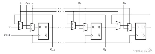
module top_module (
    input   clk,
    input   w, R, E, L,
    output  Q
);
wire     C,D;
assign C = E?w:Q;
assign D = L?R:C;
always @(posedge clk) begin
	Q <= D;
end

endmodule
DFFs and gates
给定如图所示的有限状态机电路,假设D触发器在机器开始之前最初复位为零。

module top_module (
    input    clk,
    input    x,
    output   z
);
reg    Q1,Q2,Q3;
wire   D1,D2,D3;

assign D1 = x ^ Q1;
assign D2 = x & (~Q2);
assign D3 = x | (~Q3);

always @(posedge clk) begin
	Q1 <= D1;
end

always @(posedge clk) begin
	Q2 <= D2;
end

always @(posedge clk) begin
	Q3 <= D3;
end

assign z = ~(Q1 | Q2 | Q3);

endmodule
creat circuit
实现 JK 触发器,真值表如下:

module top_module (
    input   clk,
    input   j,
    input   k,
    output  Q
);
always @(posedge clk) begin
	if (~j & ~k) begin
		Q <= Q;
	end
	else if (~j & k) begin
		Q <= 'd0;
	end
	else if (j & ~k) begin
		Q <= 'd1;
	end
	else if (j & k) begin
		Q <= ~Q;
	end
end

endmodule
Edgedetect
上升沿检测:对输入信号打一拍,打一拍的信号取反与原信号相与就可以检测出上升沿
上升沿检测:对输入信号打一拍,打一拍的信号与原信号取反相与就可以检测出上升沿
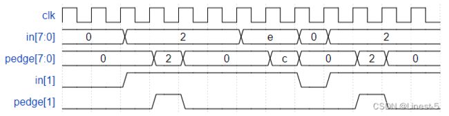
module top_module (
    input         clk,
    input  [7:0]  in,
    output [7:0]  pedge
);
reg [7:0]  in_reg;
always @(posedge clk) begin
	in_reg <= in;
end
always @(posedge clk) begin
	pedge <= in & (~in_reg);
end
endmodule
Edgedetect2
对于 8 位矢量中的每个位,检测输入信号何时从一个时钟周期变为下一个时钟周期(检测任何边沿)。输出位应在0到1转换发生后设置周期。

module top_module (
    input         clk,
    input  [7:0]  in,
    output [7:0]  anyedge
);
reg [7:0]  in_reg;
always @(posedge clk) begin
	in_reg <= in;
end
always @(posedge clk) begin
	anyedge <= in ^ in_reg;
end
endmodule
Edgecapture
对于 32 位矢量中的每个位,当输入信号在一个时钟周期内从 1 变为下一个时钟周期中的 0 时进行捕获。“捕获”意味着输出将保持1,直到寄存器复位(同步复位)。每个输出位的行为类似于SR触发器:输出位应设置为(至1)1,转换发生1至0后的周期。当复位为高电平时,输出位应在正时钟边沿复位(至0)。如果上述两个事件同时发生,则重置优先。在下面示例波形的最后4个周期中,“复位”事件发生比“set”事件早一个周期,因此这里没有冲突。
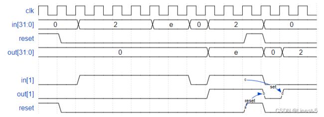
module top_module (
    input          clk,
    input          reset,
    input  [31:0]  in,
    output [31:0]  out
);
reg [31:0]  in_reg;

always @(posedge clk) begin
	in_reg <= in;
end

always @(posedge clk) begin
	if (reset) begin
		out <= 'd0;
	end
	else begin
		out <= ~in & in_reg | out;
	end
end

endmodule
Dualedge
熟悉在时钟的上升沿或时钟的下降沿触发的。双边沿触发触发器在时钟的两个边沿触发。但是,FPGA没有双边触发触发器,并且@(posedge clk or negedge clk)是不能够被综合的。构建一个在功能上表现得像双边沿触发触发器的电路:

以下提供两种方法:
module top_module (
    input   clk,
    input   d,
    output  q
);
reg   d1,d2;
always @(posedge clk) begin
	d1 <= d;
end
always @(negedge clk) begin
	d2 <= d;
end
assign q = clk?d1:d2;

endmodule

//second
module top_module (
    input   clk,
    input   d,
    output  q
);
reg   q1,q2;
always @(posedge clk) begin
	q1 <= d ^ q2;
end
always @(negedge clk) begin
	q2 <= d ^ q1;
end
assign q = q1 ^ q2;

endmodule
总结
这部分的内容比较简单,主要就是学习了创建触发器和锁存器,以及在实际设计中常用的边沿检测。