SPI
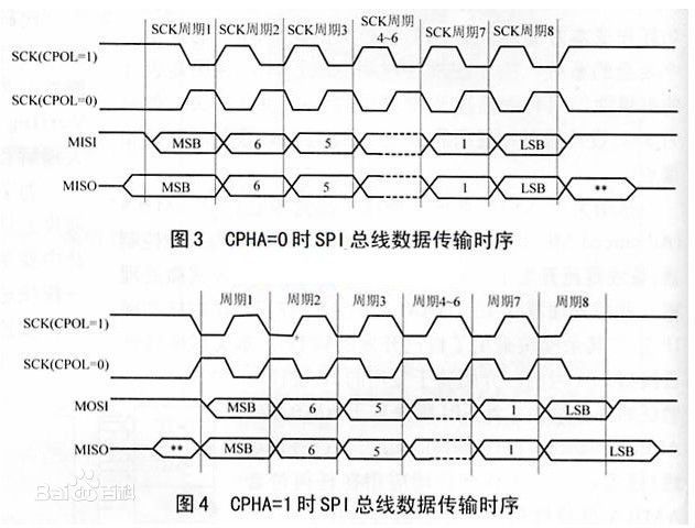
SPI模块为了和外设进行数据交换,根据外设工作要求,其输出串行同步时钟极性和相位可以进行配置。
时钟极性(CPOL)对传输协议没有重大的影响。
- 如果CPOL=0,串行同步时钟的空闲状态为低电平;
- 如果CPOL=1,串行同步时钟的空闲状态为高电平。
时钟相位(CPHA)能够配置用于选择两种不同的传输协议之一进行数据传输。
- 如果CPHA=0,在串行同步时钟的第一个跳变沿(上升或下降)数据被采样;
- 如果CPHA=1,在串行同步时钟的第二个跳变沿(上升或下降)数据被采样。
SPI主模块和与之通信的外设音时钟相位和极性应该一致。高位先传输,低位后传输。

【Clock polarity and phase】
In addition to setting the clock frequency, the master must also configure the clock polarity and phase with respect to the data. Freescale's SPI Block Guide names these two options as CPOL and CPHA respectively, and most vendors have adopted that convention.
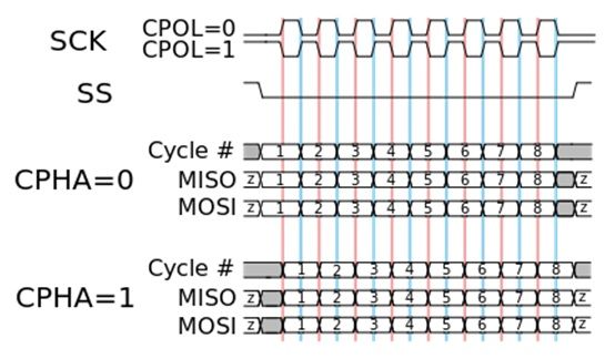
The timing diagram is shown to the right. The timing is further described below and applies to both the master and the slave device.
• At CPOL=0 the base value of the clock is zero
- For CPHA=0, data is captured on the clock's rising edge and data is propagated on a falling edge.
- For CPHA=1, data is captured on the clock's falling edge and data is propagated on a rising edge.
• At CPOL=1 the base value of the clock is one (inversion of CPOL=0)
- For CPHA=0, data is captured on clock's falling edge and data is propagated on a rising edge.
- For CPHA=1, data is captured on clock's rising edge and data is propagated on a falling edge.
That is, CPHA=0 means sample on the leading (first) clock edge, while CPHA=1 means sample on the trailing (second) clock edge, regardless of whether that clock edge is rising or falling. (CPHA=0,表明在第1个时钟跳变沿采集数据;CPHA=1,表明在第2个时钟跳变沿采集数据。)
Note that with CPHA=0, the data must be stable for a half cycle before the first clock cycle. For all CPOL and CPHA modes, the initial clock value must be stable before the chip select line goes active.(无论CPOL和CPHA是什么模式,在SS信号线有效之前,必须先初始时钟SCK线为稳定状态。)
The MOSI and MISO signals are usually stable (at their reception points) for the half cycle until the next clock transition. (MOSI和MISO在下一个时钟传输前应该保持稳定至少半个周期)
SPI master and slave devices may well sample data at different points in that half cycle.
This adds more flexibility to the communication channel between the master and slave.
Some products use different naming conventions. For example, the TI MSP430 uses the name UCCKPL instead of CPOL, and its UCCKPH is the inverse of CPHA. When connecting two chips together, carefully examine the clock phase initialization values to be sure of using the right settings.
【Timing diagram:(SPI中有关CPOL和CPHA的时序图)】
A timing diagram showing clock polarity and phase.
The red vertical line represents CPHA=0 and the blue vertical line represents CPHA=1.
