TPU Memory (1)
SOPHGO TPU-MLIR: https://tpumlir.org
Firstly, let's take a look at the brief architecture of the SOPHGO’s TPU.

We can learn from the slide that there are multiple NPU, aka Neuron Processing Unit, in the TPU, which is mainly composed of a local memory and multiple execution units. The former is used for storing data to be operated, while the latter is the smallest computing unit on the TPU. Each NPU can drive all its EUs to do one MAC operation at a time.
In terms of the overall TPU memory, it consists of system and local one. The main part of system memory is global memory, which is a DDR. Sometimes there are other components according to the special design of TPU, but we wont talk about this part here, so knowing global memory is enough for now. In terms of local memory, we only need to know it is a set of Static RAMs for now. I will further explain it later.
Typically global memory is large and is used to store the entire block of data from the host.
While local memory is limited but has the advantage of fast computation, so sometimes for a huge tensor, we need to slice it into several parts, send it to local memory for computation, then store the result back to global memory.
In order to do these operations on the TPU, we need instructions.

There are 2 main kinds of instructions:
GDMA for data transfer between system memory and local memory or within system memory
BDC is used to drive execution units to do computation work on NPU
In addition, for those calculations that are not suitable for parallel acceleration, such as NMS, SORT, we also need HAU, but this means that additional processors are required.
In terms of the physical composition of local memory, it consists of multiple Static RAMs.
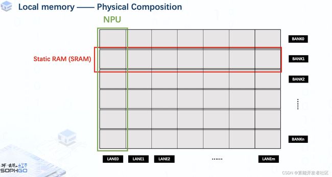
Each SRAM is called a bank.
Moreover, we divide these SRAMs into multiple parts for the same amount of NPUs and each part is called a lane.
For each NPU, it can only access to the part of local memory belongs to it, that makes execution units of a single NPU can only handle the part of tensor on its own local memory.
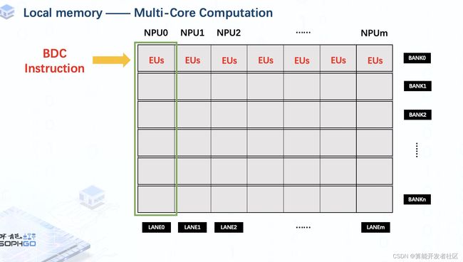
Once we call a single BDC instruction, execution units of all NPU will execute the same operation on the same location of each NPU. That’s how TPU does acceleration work.
In addition, the number of data that TPU can handle at the same time depends on number of execution unit on each NPU.
For a specific TPU, the Bytes of EU is fixed, so for data with different type, the number of EU is different.
For example, if the bytes of EU is 64, that means 64 int8 data in one NPU can be handled at the same time.

Similarly, we can calculate the corresponding EU_NUM according to the byte of the data.
For address allocation, assuming that our local memory consists of 16 SRAMs, the total local memory is 16MB, and we got 64 NPUs, so memory of each NPU is 256KB.

And the memory size of each bank in a single lane is 16KB, that equals to 16x1024 Bytes.
So the address range of this block is from 0 to 16x1024 – 1.
Similarly, the address of next bank in NPU0 starts from 16x1024 to 32x1024-1
With this principle, we can get all addresses on local memory.