【IC设计】ICC1 workshop lab guide 学习笔记
文章目录
-
- Lab1 Data Setup&Basic Flow
-
- 1.1 Create a Milkyway library
- 1.2 Load the Netlist,TLU+,Constraints and Controls
- 1.3 Basic Flow:Design Planning
- 1.4 Bsic Flow:Placement
- 1.5 Basic Flow:CTS
- 1.6 Basic Flow:Routing
- Design Planning
-
- 2.1 Load the Design
- 2.2 Initialize the Floorplan
- 2.3 Preplace the Macros Connected to I/O Pads
- 2.4 Perform Virtual Flat Placement
- 2.5 Create P/G Rings Around Macro Groups
- 2.6 Power Network Synthesis
- 2.7 Check the Timing
- 2.8 Write Out the DEF Floorplan File
- 2.9 Create 2nd Pass Design Ready for Placement
Lab1 Data Setup&Basic Flow
1.1 Create a Milkyway library
lab1_data_setup目录下有
.synopsys_dc.setup
scripts
risc_chip.mw
design_data
其中.synopsys_dc.setup中设置了若干变量,设置了搜索路径、verilog设计、sdc、def、tech_file、tlu、db库等的路径,以方便在后面使用icc时能直接调用。
启动icc_shell后会自动调用.synopsys_dc.setup,可以通过printvar来验证变量是否已设置
了解了.synopsys_dc.setup后,下面就创建设计库(即Milkyway library)
写入库的路径、库名、tf文件路径、添加reference libraries,这些都可以使用刚刚加载的变量名来替代。
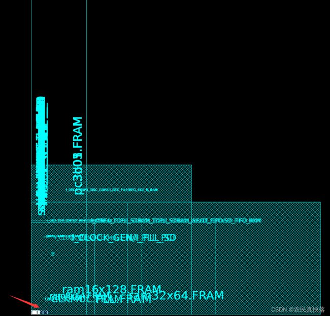
其中reference libraries需要添加ref/mw_lib/的sc、ram16x128、io三个库
这些库是Milkyway参考库:
信息是以被称为“views”的形式存储的,例如:
CEL:完整的版图信息
FRAM:用于布局布线的抽象化的版图物理信息(只有单元大小、端口名称、端口位置等简单的物理信息)
LM:带有时序和功耗信息的逻辑模型(可选*),该文件对于后端布局布线不是必须的,IC
Compiler只通过link_library变量来读取指定的(.db)格式的逻辑库。对于那些标准单元库、IO库、Memory或者其他Macro,如果设计中没有CEL View以及FRAM
View,则可以在Milkway软件中通过简单的read_lef文件的方式生成这些文件。其中lef文件全拼为:Library
Exchange Format。
创建完成后可以使用ls -a risc_chip.mw来查看库里的东西
有CEL lib lib_1 lib_bck .lock文件
总结:
这一节介绍了.synopsys_dc.setup设置了若干变量,该文件会在icc_shell启动时自动执行,进而在使用icc创建库时可以调用这些变量,无需手写。milkyway库保存了后端工作的全部信息,创建时需要指定库的存储路径,名字,参考的其他mw库,创建成功后会生成lib_name.mw,目录下有CEL,lib等文件。
涉及的相关脚本和命令:
.synopsys_dc.setup中
suppress_message是压制某些警告,我记得这个在学习java框架SpringBoot时也有相关注解,主要是告诉工具不要输出某些无所谓的警告。
history keep 100 这个应该是控制command.log记录100条最近执行的指令,缺省是20条
set_app_var和set都是设置变量 感觉区别不太大
alias是取别名,属于shell指令,把一些比较长的命令取别名为短的
lappend 变量 路径 这个含义是把该变量当做一个list,在其后增加一条路径,并和前面已有路径用空格隔开
set_min_library 没查过,无非是设置库
sdc_file是dc时可以write出来的,我感觉就是把dc设置的时序参数写出来
def_file是floor plan需要导入的
ctrl_file是opt_ctrl.tcl脚本
1.2 Load the Netlist,TLU+,Constraints and Controls
上一节创建了RISC_CHIP库,这里打开该库,导入Verilog设计(是dc出来的网表,一般命名为mapped.v或netlist.v),
然后导入TLU+文件,有3个文件
set_tlu_plus_files -max_tluplus $tlup_max \
-min_tluplus $tlup_min \
-tech2itf_map $tlup_map
关于TLU+
TLUPlus is a binary table format that stores the RC coefficients. The TLUPlus models
enable accurate RC extraction results by including the effects of width, space, density, and
temperature on the resistance coefficients. For details about modeling these effects in the
Interconnect Technology Format (ITF) file, see the StarRC documentation.
即TLU+是存放RC系数的文件。
检查物理和逻辑库的一致性、检查TLU是否已经加入:
check_library
check_tlu_plus_files
验证指定的link库已被加载
list_libs
定义power/ground的逻辑连接
source $derive_pg_file
check_mv_design -power_nets
读sdc文件 read_sdc $sdc_file
检查时序 check_timing
添加时序和优化控制
source $ctrl_file
运行零互联时延报告
保存mw_cel
总结:
这一节打开了上节创建的RISC_CHIP库,导入网表、TLU,定义了power/ground的逻辑连接,读入sdc文件,添加时序和优化控制,最后输出零互联时延报告,涉及到source脚本,各种check,还是不那么好彻底理解的。但是总体来说还是对项目进行一些基本的配置,然后输出时延报告,还没有进入到floor plan的步骤。
涉及的相关脚本和命令:
导入设计:
import_designs $verilog_file -format verilog -top $top_design
设置TLU+ :
set_tlu_plus_files -max_tluplus $tlup_max
-min_tluplus $tlup_min
-tech2itf_map $tlup_map
检查物理和逻辑库的一致性:
check_library
检查TLU+ 文件被添加,通过了检查:
check_tlu_plus_files
验证link libraries已经被加载(我的理解就是sc io ram16x128的db库
list_libs
定义power/ground的管脚和网络之间的逻辑连接
soruce $derive_pg_file #这个文件路径在./scripts/derive_pg.tcl
check_mv_design -power_nets
应用顶级设计约束
read_sdc $sdc_file
检查时序约束
check_timing
检查时序异常约束
report_timing_requirements
检查是否有路径禁用时序分析
report_disable_timing
检查设计是否被配置为特定模式或者用例
report_case_analysis
验证clocks是否被合适地建模:
report_clock
reprot_clock -skew
应用时序和优化控制
source $ctrl_file
跑0互联时序报告
source sc[TAB]z[TAB]
#The above file scripts/zic_timing.tel contains:
#set_zero_interconnect_delay_mode true
#redirect -tee zic.timing { report_timing }
#set_zero_interconnect_delay_mode false
查看zic.timing内容
exec cat zic.timing
移除理想network
remove_ideal_network [get_ports scan_en]
保存cel
save_mw_cel -as RISC_CHIP_data_setup
涉及到的脚本和命令相当多,需要查iccug,结合实践,加以理解。
1.3 Basic Flow:Design Planning
这一节提供了一个DEF格式的预定义好的floor plan file,
读入def文件,read_def $def_file
确保standard cells在power和ground metal routes之上
保存该设计cel,该文件会保存到risc_chip.mw/CEL(也就是说还是在刚刚的项目里操作)
总结:
读入预定义好的floor plan file
涉及的相关脚本和命令:
read_def $def_file
set pnet options -complete {METAL3 METAL4}
save_mw_cel -as RISC_CHIP_floorplanned
1.4 Bsic Flow:Placement
使用place_opt进行布线
分析拥塞
最后保存
总结:
疑问是,自动布线,不需要自己动手吗?那我之前上课学到的布线相关的命令是做什么的?
涉及的相关脚本和命令:
place_opt
redirect -tee place_opt.timing {report_timing}
report_congestion -grc_based -by_layer \
-routing_stage global
save_mw_cel -as RISC_CHIP_placed
1.5 Basic Flow:CTS
使用命令进行时钟树综合,然后展示时钟树。
保存cel
退出icc,discard all
总结:
似乎看着也很简单,就是几行命令搞定cts,那么后面需要自己动手试一试是否能跑的出来。
涉及的相关脚本和命令:
remove_clock_uncertainty [all_clocks]
set_fix_hold [all_clocks]
clock_opt
redirect -tee clock__opt. timing { report_timing}
save rnw cel -as RISC CHIP cts
1.6 Basic Flow:Routing
重新打开icc_shell,打开设计,选择库,重做一遍timing和optimization controls,因为这些步骤中的变量在退出icc后就没了。
然后route_opt进行自动布线
布线后输出时序报告。
保存退出
**总结:**需要对相关的命令查一下iccug,有基本的认知了解,再进行学习可能更好。
涉及的相关脚本和命令:
source $ctrl file
route opt
report_design -physical
save_mw_cel -as RISC_CHIP_routed
Design Planning
2.1 Load the Design
- 进入lab2_dp目录并打开icc_shell,
- 打开orca_lib.mw下的orca_setup cell
- Take a look at the LayoutWindow. 看看跳出的LayoutWindow
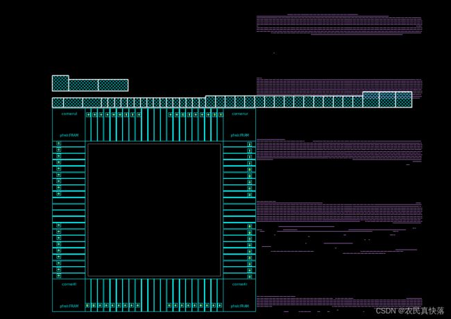
The large greenish-blue rectangles are the macro and IO pad cells, and the small purple rectangles in the lower left corner (zoom in if you want to see them more clearly), are the standard cells.
大的蓝绿色矩形是宏单元格和IO单元格,左下角的紫色小矩形(如果想看得更清楚,可以放大)是标准单元格。
All of these cells are instantiated cells in the netlist.
所有这些单元格都是网络列表中的实例化单元格。
They are all stacked on top of each other at the origin (0,0).
它们都在原点(0,0)处堆叠在一起。
Apply timing and optimization controls which are specified in ./scripts/opt_ctrl.tcl
应用在./scripts/opt_ctrl.tcl中时序和优化控制
# - - - - - - - - - - - - - - - - - - - - - - - - - - - - - - - - - - - - - - -
# General timing and optimization control settings
# - - - - - - - - - - - - - - - - - - - - - - - - - - - - - - - - - - - - - - -
set_app_var timing_enable_multiple_clocks_per_reg true
set_app_var case_analysis_with_logic_constants true
set_app_var physopt_delete_unloaded_cells false
# set physopt_power_critical_range 0.8
# set physopt_area_critical_range 0.8
set_app_var enable_recovery_removal_arcs true
# set_false_path from -to
set_fix_multiple_port_nets -all -buffer_constants
set_auto_disable_drc_nets -constant false
set_timing_derate -max -early 0.95
# set_dont_use Most of these settings are discussed in the Appendix of Unit 1. Some are discussed in later Units. Do not spend time here trying to
understand them
这些设置大多数在第一单元的附录中讨论过。其中一些将在后面的单元中讨论。不要在这里花时间试图去理解它们。
2.2 Initialize the Floorplan
16、大概阐述下做floorplan的步骤?
- Create physical-only pad cell(PG cell,corner cell), specify pad cell location
- Create floorplan(设置好die size和core area)
- Insert pad filler
- Place macros
- Apply placement blockage
- 添加physical only cells(tap cell, endcap cell, decap cell)
- Build power network
- 对于多电压域设计还要create voltage area等等
The logical netlist from synthesis does not contain physical-only cells such as power and ground pad cells or corner pad cells. You have to therefore create these extra cells before being able to physically place them in the periphery area of your chip.
来自综合的逻辑网表不包含物理单元,如电源和接地单元或角落单元。你需要先创建这些单元,然后才能在芯片的外围区域摆放。
Create the corner and P/G cells and define all pad cell positions using a provided script
创建这些角单元和P/G单元,并使用一个提供的脚本来定义所有pad cell。
Hint:When typing use the [Tab] key for command/option/file completion.
输入时使用Tab键来补全命令/选项/文件
source –echo scripts/pad_cell_cons.tcl
# Create corners and P/G pads
create_cell {cornerll cornerlr cornerul cornerur} pfrelr
create_cell {vss1left vss1right vss1top vss1bottom} pv0i
create_cell {vdd1left vdd1right vdd1top vdd1bottom} pvdi
create_cell {vss2left vss2right vss2top vss2bottom} pv0a
create_cell {vdd2left vdd2right vdd2top vdd2bottom} pvda

# Define corner pad locations
set_pad_physical_constraints -pad_name "cornerul" -side 1
set_pad_physical_constraints -pad_name "cornerur" -side 2
set_pad_physical_constraints -pad_name "cornerlr" -side 3
set_pad_physical_constraints -pad_name "cornerll" -side 4

# Define signal and PG  pad locations

# Left side
set_pad_physical_constraints -pad_name "pad_iopad_0" -side 1 -order 1
set_pad_physical_constraints -pad_name "pad_iopad_1" -side 1 -order 2
set_pad_physical_constraints -pad_name "pad_iopad_2" -side 1 -order 3
set_pad_physical_constraints -pad_name "pad_iopad_3" -side 1 -order 4
set_pad_physical_constraints -pad_name "pad_iopad_4" -side 1 -order 5
set_pad_physical_constraints -pad_name "pad_iopad_5" -side 1 -order 6
set_pad_physical_constraints -pad_name "pad_iopad_6" -side 1 -order 7
set_pad_physical_constraints -pad_name "pad_iopad_7" -side 1 -order 8
set_pad_physical_constraints -pad_name "pad_iopad_8" -side 1 -order 9
set_pad_physical_constraints -pad_name "vdd2left" -side 1 -order 10
set_pad_physical_constraints -pad_name "vdd1left" -side 1 -order 11
set_pad_physical_constraints -pad_name "vss1left" -side 1 -order 12
set_pad_physical_constraints -pad_name "vss2left" -side 1 -order 13
set_pad_physical_constraints -pad_name "pad_iopad_9" -side 1 -order 14
set_pad_physical_constraints -pad_name "pad_iopad_10" -side 1 -order 15
set_pad_physical_constraints -pad_name "pad_iopad_11" -side 1 -order 16
set_pad_physical_constraints -pad_name "pad_iopad_12" -side 1 -order 17
set_pad_physical_constraints -pad_name "pad_iopad_13" -side 1 -order 18
set_pad_physical_constraints -pad_name "pad_iopad_14" -side 1 -order 19
set_pad_physical_constraints -pad_name "pad_iopad_15" -side 1 -order 20
set_pad_physical_constraints -pad_name "pclk_iopad" -side 1 -order 21
set_pad_physical_constraints -pad_name "pll_bypass_iopad" -side 1 -order 22

# Top side
set_pad_physical_constraints -pad_name "pc_be_iopad_0" -side 2 -order 1
set_pad_physical_constraints -pad_name "pc_be_iopad_1" -side 2 -order 2
set_pad_physical_constraints -pad_name "pc_be_iopad_2" -side 2 -order 3
set_pad_physical_constraints -pad_name "pc_be_iopad_3" -side 2 -order 4
set_pad_physical_constraints -pad_name "pdevsel_n_iopad" -side 2 -order 5
set_pad_physical_constraints -pad_name "pframe_n_iopad" -side 2 -order 6
set_pad_physical_constraints -pad_name "pgnt_n_iopad" -side 2 -order 7
set_pad_physical_constraints -pad_name "pidsel_iopad" -side 2 -order 8
set_pad_physical_constraints -pad_name "pirdy_n_iopad" -side 2 -order 9
set_pad_physical_constraints -pad_name "vdd2top" -side 2 -order 10
set_pad_physical_constraints -pad_name "vdd1top" -side 2 -order 11
set_pad_physical_constraints -pad_name "vss1top" -side 2 -order 12
set_pad_physical_constraints -pad_name "vss2top" -side 2 -order 13
set_pad_physical_constraints -pad_name "ppar_iopad" -side 2 -order 14
set_pad_physical_constraints -pad_name "pperr_n_iopad" -side 2 -order 15
set_pad_physical_constraints -pad_name "preq_n_iopad" -side 2 -order 16
set_pad_physical_constraints -pad_name "prst_n_iopad" -side 2 -order 17
set_pad_physical_constraints -pad_name "pstop_n_iopad" -side 2 -order 18
set_pad_physical_constraints -pad_name "pserr_n_iopad" -side 2 -order 19
set_pad_physical_constraints -pad_name "ptrdy_n_iopad" -side 2 -order 20
set_pad_physical_constraints -pad_name "sys_clk_iopad" -side 2 -order 21
set_pad_physical_constraints -pad_name "sdr_clk_iopad" -side 2 -order 22

# Right side
set_pad_physical_constraints -pad_name "sdram_A_iopad_0" -side 3 -order 1
set_pad_physical_constraints -pad_name "sdram_A_iopad_1" -side 3 -order 2
set_pad_physical_constraints -pad_name "sdram_A_iopad_2" -side 3 -order 3
set_pad_physical_constraints -pad_name "sdram_A_iopad_3" -side 3 -order 4
set_pad_physical_constraints -pad_name "sdram_A_iopad_4" -side 3 -order 5
set_pad_physical_constraints -pad_name "sdram_A_iopad_5" -side 3 -order 6
set_pad_physical_constraints -pad_name "sdram_A_iopad_6" -side 3 -order 7
set_pad_physical_constraints -pad_name "sdram_A_iopad_7" -side 3 -order 8
set_pad_physical_constraints -pad_name "sdram_A_iopad_8" -side 3 -order 9
set_pad_physical_constraints -pad_name "vdd2right" -side 3 -order 10
set_pad_physical_constraints -pad_name "vdd1right" -side 3 -order 11
set_pad_physical_constraints -pad_name "vss1right" -side 3 -order 12
set_pad_physical_constraints -pad_name "vss2right" -side 3 -order 13
set_pad_physical_constraints -pad_name "sdram_A_iopad_9" -side 3 -order 14
set_pad_physical_constraints -pad_name "sdram_BWS_iopad_0" -side 3 -order 15
set_pad_physical_constraints -pad_name "sdram_BWS_iopad_1" -side 3 -order 16
set_pad_physical_constraints -pad_name "sdram_LD_iopad" -side 3 -order 17
set_pad_physical_constraints -pad_name "sdram_RW_iopad" -side 3 -order 18
set_pad_physical_constraints -pad_name "powersave_iopad" -side 3 -order 19
set_pad_physical_constraints -pad_name "scan_en_iopad" -side 3 -order 20
set_pad_physical_constraints -pad_name "pm66en_iopad" -side 3 -order 21
set_pad_physical_constraints -pad_name "test_mode_iopad" -side 3 -order 22

# Bottom side
set_pad_physical_constraints -pad_name "sdram_CK_iopad" -side 4 -order 1
set_pad_physical_constraints -pad_name "sdram_CKn_iopad" -side 4 -order 2
set_pad_physical_constraints -pad_name "sdram_DQ_iopad_0" -side 4 -order 3
set_pad_physical_constraints -pad_name "sdram_DQ_iopad_1" -side 4 -order 4
set_pad_physical_constraints -pad_name "sdram_DQ_iopad_2" -side 4 -order 5
set_pad_physical_constraints -pad_name "sdram_DQ_iopad_3" -side 4 -order 6
set_pad_physical_constraints -pad_name "sdram_DQ_iopad_4" -side 4 -order 7
set_pad_physical_constraints -pad_name "sdram_DQ_iopad_5" -side 4 -order 8
set_pad_physical_constraints -pad_name "sdram_DQ_iopad_6" -side 4 -order 9
set_pad_physical_constraints -pad_name "vdd2bottom" -side 4 -order 10
set_pad_physical_constraints -pad_name "vdd1bottom" -side 4 -order 11
set_pad_physical_constraints -pad_name "vss1bottom" -side 4 -order 12
set_pad_physical_constraints -pad_name "vss2bottom" -side 4 -order 13
set_pad_physical_constraints -pad_name "sdram_DQ_iopad_7" -side 4 -order 14
set_pad_physical_constraints -pad_name "sdram_DQ_iopad_8" -side 4 -order 15
set_pad_physical_constraints -pad_name "sdram_DQ_iopad_9" -side 4 -order 16
set_pad_physical_constraints -pad_name "sdram_DQ_iopad_10" -side 4 -order 17
set_pad_physical_constraints -pad_name "sdram_DQ_iopad_11" -side 4 -order 18
set_pad_physical_constraints -pad_name "sdram_DQ_iopad_12" -side 4 -order 19
set_pad_physical_constraints -pad_name "sdram_DQ_iopad_13" -side 4 -order 20
set_pad_physical_constraints -pad_name "sdram_DQ_iopad_14" -side 4 -order 21
set_pad_physical_constraints -pad_name "sdram_DQ_iopad_15" -side 4 -order 22
Look at the log output to verify that these cells have been created and constrained without any error or warning messages.
查看日志输出,以验证这些单元格是否已经创建和约束,没有任何错误或警告信息。
In a separate UNIX window look at the above script to help you answer the following questions. Check your answers against the solution in the back.
在一个单独的unix窗口中查看上面的脚本,以帮助您回答以下问题。对照后面的答案检查你的答案。
Q1.1
What is the command to create a pad cell called VDD_TEST using the reference cell pvdi? (Do not run this command!)
使用参考单元pvdi创建名为VDD_TEST的pad单元的命令是什么?(不要运行这个命令!)
create_cell {VDD_TEST} pvdi
man查询create_cell部分结果:
The following example creates leaf cells using library cells as
references.
prompt> create_cell {U3 U4} my_lib/NAND2
prompt> create_cell “U5” my_lib/NOR2
Q1.2
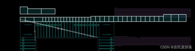
What “side” is used to define the location of the upper-right corner cell (cornerur)?
哪个“边”用于定义右上角单元格(拐角)的位置?
man这个命令部分结果:
   -side side_number
          Specifies  the  die  edge on which the pad must reside. Pads are
          supported for rectangular floorplans only. The valid values  for
          this option are
          指定die的边缘在pad的位置,pad只支持矩形的floor paln,合法参数有:

          o 0 (default - no side constraints)

          o 1 (left side constraint)

          o 2 (top side constraint)

          o 3 (right side constraint)

          o 4 (bottom side constraint)

          The  default is 0, which means that the pad does not have a side
          constraint.
          默认是0,意味着pad没有边的约束

   -order order_number
          Specifies the placement order number for the pad. The  placement
          order  is  a  clockwise ordering constraint for the left and top
          sides. The placement order is a counterclockwise  ordering  con-
          straint  for the right and bottom sides. The order argument must
          be a positive integer.
          指定这个pad的布局顺序,布局顺序是从左上角开始顺时针数的。

          The default is 0, which means that the  pad  does  not  have  an
          ordering constraint.
          默认是0,意味着pad没有顺序约束
个人总结:
我的理解是这样的,side为1~4分别指定的是pad在芯片的左、上、右、下,而order指定了在side确定的情况下,pad的顺序。
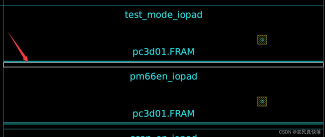
如图所示,我们将红框内放大,可以看到pad的具体名称。
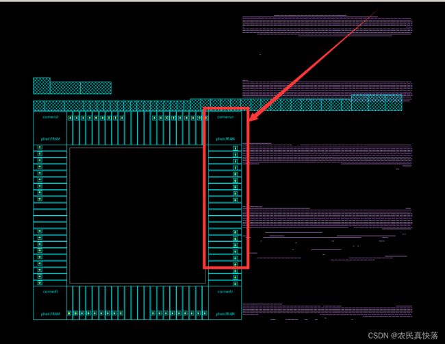
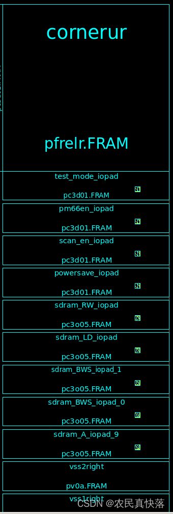
其中test_mode_iopad在最上面,是order最大的,即对应命令
set_pad_physical_constraints -pad_name "test_mode_iopad" -side 3 -order 22
可以得出结论,order的顺序是左下角最小,从左往后以此增大,从上往下依次增大,即坐标轴的递增关系。
Initialize the floorplan:
Select Floorplan Initialize Floorplan…
Change the Core utilization to 0.8 (80%).
Change the Core to left/right/bottom/top spacing to 30.
Click OK.
这一段无需翻译
- Fit [F] the LayoutWindow and have a look at the chip’s core and periphery
areas. The blue hash-marked rectangles outside the chip along the top edge are
the unplaced macro cells. The purple objects along the right edge are all the
standard cells.
蓝色带散列标记的矩形是未布局的宏单元,右边缘紫色的是标准单元。
Note: The corner cells are easily visible – look at the large blue
square that takes up the full layout view (labeled pfrelr).
There are four groups of four P/G pads placed in the middle
of each side
注意:边角单元格很容易看到——看看占据整个布局视图的蓝色大方块(标记为pfrelr)。
有四组四个P/G放置在每边的中间。
个人总结:
图中蓝色的是macro cell,紫色的是std cell,图中的macro cell有3类,一类是corner cell,在四个角,一类是iopad,占据大部分,最后是vdd和vss,用作供电和接地。我现在认为这里的pad其实只是个框,方便后面布局放入真正的元件,目前并没有物理上的实际功能。
-
Zoom into the periphery area of the chip and notice that the spacing between
all the pads is about equal
放大到芯片的外围区域,注意到所有pad之间的间距大约相等 -
Insert the pad fillers to fill the gaps between the pads.
插入pad fillers来填补pad之间的gap
Depending on the technology and library being used, this may be needed for N- or P-well and/or for power/ground pad ring continuity.
根据所使用的技术和库,这可能需要用于P/N well或P/G pad ring continuity。
To keep the number of pad filler cells required to a minimum, specify the larger filler cells first in the list.
要将所需的填充单元格数量保持在最小值,先在列表中指定较大的filler单元。
Otherwise,a 1,000 um space will get filled with 200 x 5 um width cells, instead of one 1,000 um width cell. Enter the command in the box below or source the provided script scripts/insert_pad_filler.tcl
否则,一个1000um的空间将被200个5um的单元填满,而不是1个1000um宽度的单元。在下方的方框中输入命令,或者使用提供的脚本
scripts/insert_pad_filler.tcl
insert_pad_filler –cell "pfeed10000 pfeed05000 \
pfeed02000 pfeed01000 pfeed00500 pfeed00200 \
pfeed00100 pfeed00050 pfeed00010 pfeed00005"
man insert_pad_filler的部分结果:
ARGUMENTS
-cell lib_cells
Specifies the names of the pad filler cells to be used. The
tool adds the cells in the priority that they are specified.
也就是说,字符串中的序列就是优先级顺序,尽可能用大的filler,以减少填充的filler数量。
-
Zoom into the space between two pad cells and notice the filler cells that have
been inserted.
放大两个pad cell之间的空间,注意到filler cell已经被插入了。
-
Make the “logical” connection (no physical routing) between the
power/ground signals and all power/ground pins of the I/O pads, macros and
standard cells, by executing the following script:
通过执行以下脚本,在P/G信号和I/O pad,macro和std cell之间建立逻辑连接
source –echo scripts/connect_pg.tcl
Note: There are 3 different power supplies in this design: VDD,
VDDQ and VDDO. The latter two are used in the periphery
of the chip.
**注意:**本设计有3种不同的电源VDD VDDQ VDDO,后两个用在芯片的外围。
- Build the PAD area power supply ring: create_pad_rings
创建PAD区域电源环:create_pad_rings
Zoom into the area between the pads to see that metal routes have been added, over the filler cells, to connect the existing power routes within each pad cell to form continuous P/G pad rings.
放大PAD之间的区域,可以看到在填充单元上已经添加了金属线路,以连接每个PAD单元内现有的电源路由,形成连续的P/G PAD环。
- Save the design as “floorplan_init”:
save_mw_cel –as floorplan_init
2.3 Preplace the Macros Connected to I/O Pads
In this task you will identify the macros that are connected to I/O pad cells and you
will manually place them in the core area such that their connections to the I/O pads
are as short as possible.
在本任务中,您将识别连接到I/O pad单元的宏,并将它们手动放置在核心区域中,以便它们与I/O pad的连接尽可能短。
- Zoom in to see the top periphery area shown in Figure 1 below.
- Identify macros that connect to I/O pads, as follows:
Choose Select Cells By Types…
Click the Uncheck All button in the top (Cell Type) section of the dialog box.
Select the Macro cell type check box.
Click the Select All button in lower left corner of the dialog box.
Click OK.
Notice that all the macros are now selected – highlighted in white.