Latch up (闩锁效应)
Latch-up
latch up 是指cmos晶片中, 在电源power VDD和地线GND(VSS)之间由于寄生的PNP和NPN双极性BJT(Bipolar Junction Transistors)相互影响而产生的一低阻抗通路, 它的存在会使VDD和GND之间产生大电流,损坏MOS管。
In the simplest way, the latch-up issue can be defined as a formation of a direct path from VDD to GND terminal in the design, which will cause a huge current flow between the power and ground terminal.
态
-
Latch-up发生的条件:
- 当两个BJT都导通,在VDD和GND之间产生低阻抗通路(low impedance path between the power and ground terminals.),High resistance of n-well and p-substrate
- 两个晶体管反馈回路(feedback loop)增益的乘积大于1,β1 x β2 > 1
-
Latch-up产生原因:
- Noise at the output terminal,the output voltage has gone beyond/below the VDD due to noise. 输出电压(I/O的信号)高于VDD电压,芯片产生大电流,导致latch-up;
- ESD (Electrostatic Discharge) event,可能会从保护电路中引入少量带电载流子到阱或衬底中
- Ionizing radiation(电离辐射)
当无外界干扰未引起触发时,两个BJT处于截止状态
Latch-up Prevention in CMOS Logics
Once the latch-up occurred in CMOS design, lots of current start flowing directly from VDD to GND and will cause the failure of chip. So we must protect our chip from latch-up. In the next article, we will discuss the method to prevent the latch-up issue.
- n-well and p-substrate resistance can be reduced by increasing the doping but it will degrade the device performance drastically.
- But we can cut down the gains of parasitic BJT (β) and prevent the latch-up issue.
-
P(PMOS的Source/Drain)— N(PMOS的N well)—P(P sub)
- QPNP为一垂直式PNP BJT, 基极(base)是nwell, 基极到集电极(collector)的电流增益 β1 可达数百倍
-
N(PMOS的N well) — P(P sub) — **N(NMOS的Source/Drain )**形成两个BJT
- QNPN是一侧面式的NPN BJT,基极为P substrate,基极到集电极(collector)的电流增益 β2可达数十倍
-
Qp和Qn 的基级连接了对方的集电极,形成了一个正反馈的回路,经过多轮正反馈,NW和PW出现了一条低阻抗的通路,导致VDD和VSS之间出现大电流,永久性损坏MOS管

防止latch up
- n-well and p-substrate resistance can be reduced by increasing the doping but it will degrade the device performance drastically.
- But we can cut down the gains of parasitic BJT (β) and prevent the latch-up issue.
- Guard ring
- Well tap cells
- Isolation trench(氧化物隔离槽(oxide trench)和掩埋氧化物(buried oxide))
- Epitaxial layer(外延层)
- Retrograde well doping
- Combination of epitaxial layer and retrograde well doping
- FDSOI Technology
- ESD protection techniques
- ESD 电路的设计需要足够健壮,防止ESD 电流没有被通过设定的通路泄放掉,流入内部电路,导致内部电路的电势被突然抬高,满足latch up 条件并触发。
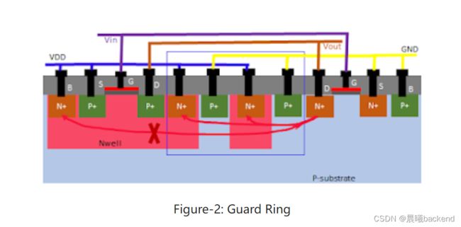
Guard ring
-
If Vout goes below the VSS and the diode between drain and p-substrate of nMOS become forward bias, electrons from drain start injecting from to substrate and collected by the body of pMOS. This cause a current from in the opposite direction of electron flow. which ultimately triggers the Qp transistor as shown in the figure-1. Now to break this chain, two sets of n+ implant in n-well, p+ implant on p-substrate added in between nMOS and nMOS as shown in the figure-2. These will collect the
electronsinjected from thedrain of nMOSandprevent the current flow from the drain of nMOS to the body of pMOS. Which stops triggering the Qp BJT. -
Similarly in case of the Vout goes above the VDD and drain of pMOS start injecting holes in n-well and goes and collected by the body of nMOS. This lead to the trigger of Qn BJT. But by adding the guard ring these holes will be collected by the guard ring and stop the latch-up.
Well tap cells
- 在IO的周围添加足够数量的tapcell,使内部电路抬起的电势能够被tap 到VDD或者VSS,tsmc 对IO周边的tapcell的摆放有相应的约束要求。
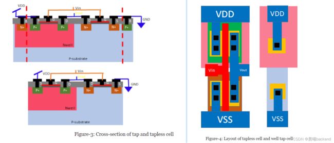
In tapless standard cell design to prevent the latch-up, we need to tap the n-well to VDD and p-sub to VSS. These well tap cells tap the n-well to VDD and p-sub to VSS. Figure-3 shows the crosssection of tapless cell and figure-4 show the layout of well tap cell and tapless standard cell.
- The well tap cells are placed in the standard cell row in the regular interval as per the maximum distance rule define in technology library.
Oxide trench isolation
- 使用氧化物隔离槽(oxide trench)和掩埋氧化物(buried oxide)层隔离NMOS和PMOS器件
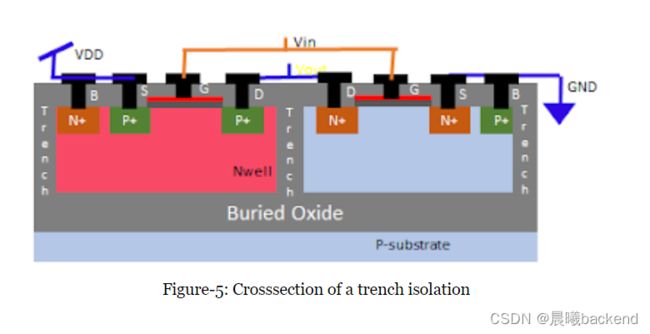
- In this technique, nMOS and pMOS have insolated using the buried oxide and oxide trench. A horizontal buried oxide created deep inside and vertical oxide trenches are created later and connected both together to separate the n-well and p-substrate. The oxide trenches are
isolatorin nature so oxide trench stops the formation of the PNPN device. A cross-section of oxide trench isolation is shown in the figure-5.
Epitaxial layer(外延层)

- In this technique, a low doped p-epitaxial layer (known as P-) grown over the P-substrate (called P+). The P- epitaxial layer provides a low impedance path for minority carrier which prevents the latch-up triggering. This technique is also called P on P+. A cross-section epitaxial layer has shown in the figure-6.
- The only problem with this technique is, it’s a sophisticated process to grow the epitaxy layer. Another alternative is we can use the epitaxy wafer for this purpose.
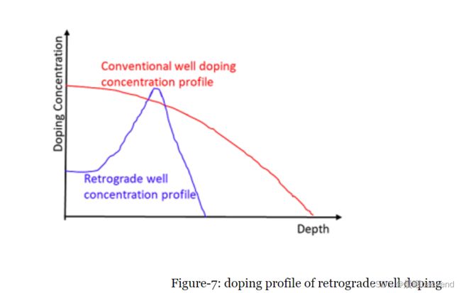
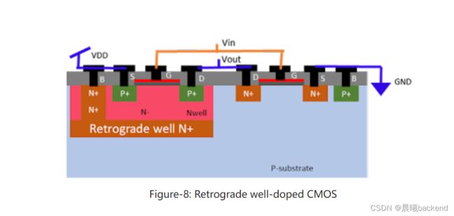
Retrograde well doping (N-表示低浓度参杂)
- In normal n-well doping process, the doping concentration is highest at the surface and it decreases as the depth of well increases. But in the retrograde well doping process, there is very precise control of doping concentration over the depth and we have peak doping concentration at deep inside the n-well, not at the surface. A doping profile of normal doping and retrograde well doping is shown in figure-7.
- A retrograde well doping is done at the bottom of normal n-well as shown in the figure-8. This region has a high doping concentration and creates a low resistance path. The body connection which is taken from N+ doping is extended to this high dopped region. So there is the formation of low resistive path bellow the n-well which stops the triggering of PNPN device. A cross-section view of retrograde well doping has shown in figure-8.
Combination of epitaxial layer and retrograde well doping
- We can use a combination of the epitaxial layer and retrograde well doping together both the techniques together which is also a very effective way to prevent the latch-up issue but the process is a bit complex.
SOI Technology

-
In SOI (Silicon on Insulator) technology an oxide layer comes below the source-drain doping and stop the parasitic BJTs formation. So SOI technology completely eliminates the latch-up issue. A cross-section of CMOS in SOI technology has shown in figure-9.
-
We can use a combination of the epitaxial layer and retrograde well doping together both the techniques together which is also a very effective way to prevent the latch-up issue but the process is a bit complex.
- These are the ways to prevent latch-up in CMOS technology. Each technique has its own progressive and conservative