牛客网Verilog刷题 | 入门特别版本
文章目录
- 1、 VL1 输出1
- 2、VL2 wire连线
- 3、 VL3 多wire连接
- 4、VL4 反相器
- 5、VL5 与门
- 6、VL6 NOR 门
- 7、VL7 XOR 门
- 8、VL8 逻辑运算
- 10、VL10 逻辑运算2
- 11、VL11 多位信号
- 12、VL12 信号顺序调整
- 13、VL13 位运算与逻辑运算
- 14、VL14 对信号按位操作
- 15、VL15 信号级联合并
- 16、VL16 信号反转输出
- 17、VL17 三元操作符
1、 VL1 输出1
描述
构建一个没有输入和一个输出常数1的输出的电路
输入描述:
无
输出描述:
输出信号为one
`timescale 1ns/1ns

module top_module(
    output  one
);

assign one = 1;

endmodule
2、VL2 wire连线
描述
创建一个具有一个输入和一个输出的模块,其行为类似于电路上的连线。
输入描述:
输入信号in0
输出描述:
输出信号out1
`timescale 1ns/1ns

module wire0( input in0, output out1

);
    assign out1 = in0;
endmodule
3、 VL3 多wire连接
描述
创建一个具有 2个输入和 3个输出的模块,使用线连接的方式:
a -> z
b -> x
b -> y
输入描述:
input wire a b
输出描述:
output wire x y z
`timescale 1ns/1ns

module top_module(

  a, b, x, y, z

);
    input  a, b;
    output x, y, z;
    assign x = b;
    assign y = b;
    assign z = a;

endmodule
4、VL4 反相器
描述
输出输入信号的值的相反的值
输入描述:
in
输出描述:
out
`timescale 1ns/1ns

module top_module(
   	input in,
	output out
);
	assign out = ~in;
endmodule
5、VL5 与门
描述
创建实现 AND 门的模块,输入有三个wire,将三个信号(a b c)进行与操作,请思考在实际电路需要几个与门?请写出对应的RTL
输入描述:
a b c
输出描述:
d
`timescale 1ns/1ns
module top_module(
    input a,
    input b,
    input c,
    output d );

    assign d = a & b & c;

endmodule
6、VL6 NOR 门
描述
创建实现 OR和NOR 的模块,NOR 门是输出反相的 OR 门。
c 是 nor输出,d是or输出
输入描述:
a b
输出描述:
c d
`timescale 1ns/1ns

module top_module(
    input a,
    input b,
    output c,
    output d);

    assign c = a ~| b;
    assign d = a | b;

endmodule
7、VL7 XOR 门
描述
创建一个实现 XOR 门的模块
输入描述:
a b
输出描述:
c
`timescale 1ns/1ns

module top_module(
    input a,
    input b,
    output c );

    assign c = a ^ b;

endmodule
8、VL8 逻辑运算
描述
写出如图的rtl逻辑,限制使用最多四次assign
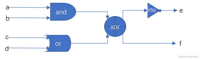
输入描述:
a b c d
输出描述:
e f
`timescale 1ns/1ns

module top_module (
	input a,
	input b,
	input c,
	input d,
	output e,
	output f );

	wire out_xor;
	assign out_xor = (a & b) ^ (c | d);
	assign e = ~out_xor;
	assign f = out_xor;

endmodule
9、VL9 模拟逻辑芯片
描述
下图为某芯片的逻辑,请通过RTL实现它的功能

输入描述:
p1a, p1b, p1c, p1d, p1e, p1f,p2a, p2b, p2c, p2d
输出描述:
p1y,p2y
`timescale 1ns/1ns

module top_module (
    input p1a, p1b, p1c, p1d, p1e, p1f,
    output p1y,
    input p2a, p2b, p2c, p2d,
    output p2y );

    assign p1y = (p1a & p1b & p1c) | (p1f & p1e & p1d);
    assign p2y = (p2a & p2b) | (p2c & p2d);
endmodule
10、VL10 逻辑运算2
描述
根据下述逻辑,给出对应的module设计
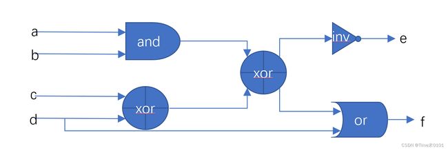
输入描述:
a b c d
输出描述:
e f
`timescale 1ns/1ns

module top_module (
	input a,
	input b,
	input c,
	input d,
	output e,
	output f );

	wire out_xor;
	assign out_xor = (a & b) ^ (c ^ d);
	assign e = ~out_xor;
	assign f = out_xor | d;
endmodule
11、VL11 多位信号
描述
构建一个具有一个3位输入in的信号[2:0],将其分成三个独立的输出a b c(从2到0)
输入描述:
in
输出描述:
a b c
`timescale 1ns/1ns

module top_module(
    in, a, b, c
);

    input [2:0] in;
    output a, b, c;
    assign a = in[2];
    assign b = in[1];
    assign c = in[0];

endmodule
12、VL12 信号顺序调整
描述
一个16位信号in包含四个四位数[3:0]a[3:0]b[3:0]c[3:0]d,将它们顺序倒置为dcba输出,输出out
输入描述:
in
输出描述:
out
`timescale 1ns/1ns

module top_module(
    in, out
);
    input [15:0] in;
    output [15:0] out;
    assign out = { in[3:0], in[7:4], in[11:8], in[15:12] };
endmodule
13、VL13 位运算与逻辑运算
描述
现有一个模块,输入信号为[2:0]a和[2:0]b,请输出信号的按位或[2:0]c和或信号d
输入描述:
[2:0]a [2:0]b
输出描述:
[2:0]c d
`timescale 1ns/1ns

module top_module(
	input [2:0] a,
	input [2:0] b,
	output [2:0] c,
	output d
);

	assign c = a | b;
	assign d = a || b;
endmodule
14、VL14 对信号按位操作
描述
将一个五输入的信号分别进行的每一位进行: 全部按位与;全部按位或;全部按位异或
输入描述:
[4:0]in
输出描述:
out_and, out_or, out_xor
`timescale 1ns/1ns

module top_module(
    input [4:0] in,
    output out_and,
    output out_or,
    output out_xor
);
    assign out_and = & in;
    assign out_or = | in;
    assign out_xor = ^ in;
endmodule
15、VL15 信号级联合并
描述
将6个输入信号串联转为四个信号输出,输入信号为[4:0] a[4:0] b[4:0]c [4:0]d [4:0]e [4:0]f,末尾增加一个宽度为两位的3,形成32位长度后,按照从前到后的顺序输出[7:0]w [7:0]x [7:0]y [7:0]z
输入描述:
[4:0] a[4:0] b[4:0]c [4:0]d [4:0]e [4:0]f
输出描述:
[7:0]w [7:0]x [7:0]y [7:0]z
在`timescale 1ns/1ns

module top_module(
    input [4:0] a, b, c, d, e, f,
    output [7:0] w, x, y, z );
    assign { w, x, y, z } = {a, b, c, d, e, f, 2'b11};
endmodule
16、VL16 信号反转输出
描述
输入一个16位的信号in,将其从低位到高位输出(即反转顺序输出)为out
输入描述:
[15:0] in
输出描述:
[15:0] out
`timescale 1ns/1ns

module top_module(
    input [15:0] in,
	output [15:0] out
);
    reg [15:0] out;
    integer i;
    always@(*)begin
        for(i=0; i<=15; i=i+1) begin
            out[15-i] = in[i];
        end
    end
endmodule
个人完成90%,这里一开始用initial总是不成功
需要搞清楚 always 和initial的用法。
17、VL17 三元操作符
描述
给定四个无符号数字,找到最大值。不使用if进行判断,尽量少使用语句的情况下完成。
输入描述:
[7:0]a b c d
输出描述:
[7:0] max
`timescale 1ns/1ns

module top_module(
    input [7:0] a, b, c, d,
    output [7:0] max);

        assign max = (((a >= b) ? a:b)>=((c>=d)? c:d)) ?((a >= b) ? a:b):((c>=d) ? c:d);

endmodule
注:一开始分开比较测试但就是 不用过,最后干脆就直接一行搞定,既然尽量少使用语句,那就一行。