【原创】The solutional manual of the Verilog HDL: A Guide to Digital Design and Synthesis (2nd)--ch10
Chapter 10. Timing and Delays
10.6 Exercises
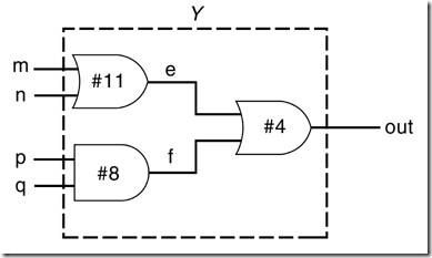
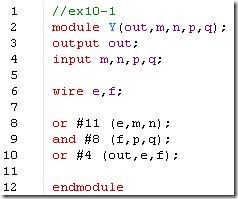
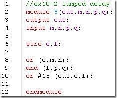
1. What type of delay model is used in the following circuit? Write the Verilog description for the module Y.
my answer:
Distributed Delay.
2. Use the largest delay in the module to convert the circuit to a lumped delay model. Using a lumped delay model, write the Verilog description for the module Y.
my answer:
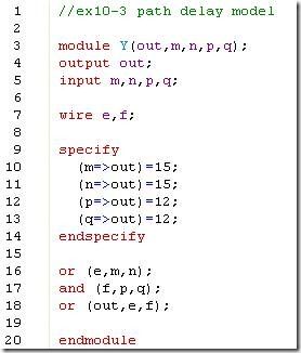
3. Compute the delays along each path from input to output for the circuit in Exercise 1. Write the Verilog description, using the path delay model. Use specify blocks.
my answer:
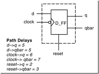
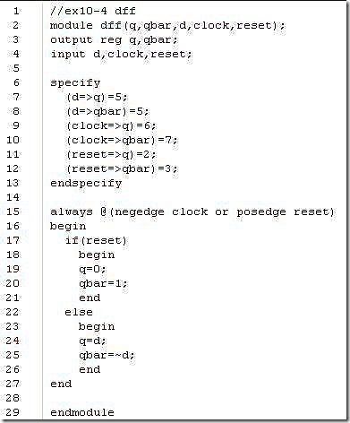
4. Consider the negative edge-triggered with the asynchronous reset D-flipflop shown in the figure below. Write the Verilog description for the module D_FF. Show only the I/O ports and path delay specification. Describe path delays, using parallel connection.
my answer:
5. Modify the D-flipflop in Exercise 4 if all path dealys are 5 units. Describe the path delays, using full connections to q and qbar.
my answer:
6. Assume that a six-delay specification is to be specified for all path delays. All path delays are equal. In the specify block, define parameters t_01=4,t_10=5,t_0z=7,t_z1=2,t_1z=3,t_z0=8. Use the D-flipflop in Exercise 4 and write the six-delay specification for all paths, using full connections.
my answer:
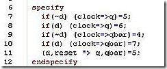
7. In Exercise 4,modify the delay specification for the D-flipflop if the delays are dependent on the value of d as follws:
clock -> q = 5 for d = 1'b0, clock -> q= 6 otherwise
clock -> qbar = 4 for d = 1'b0, clock ->qbar = 7 otherwise
All other delays are 5 units.
my answer:
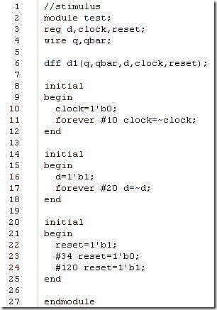
8. For the D-flipflop in Exercise 7, add timing checks for the D_flipflop in the specify block as follows:
The minimum setup time for d with respect to clock is 8.
The minimum hold time for d with respect to clock is 4.
The reset signal is active high. The minimum width of a reset pulse is 42.
my answer:
9. Describe delay back-annotation. Draw the flow diagram for delay back-annotation.
Reference
Smair Palnitkar, <Verilog HDL: A Guide to Digital Design and Synthesis (2nd) >
