OpenRisc-32-ORPSoC烧写外部spi flash
引言
经过前面的分析和介绍,我们对ORPSoC的启动过程(http://blog.csdn.net/rill_zhen/article/details/8855743)和
ORpSoC的debug子系统(http://blog.csdn.net/rill_zhen/article/details/9045837)有了初步的了解,
但是对于启动和debug前的工作还没有仔细分析过。比如FPGA是怎么config的,orpmon是怎么load的,是如何事先烧到外部的flash里的,等等。
本小节就试图解决这个问题,但是没有成功,就作为最终解决问题的参考吧。
1,系统的setup
1>回顾
根据前面的分析,我们知道了ORPSoC复位之后的操作,简单整理如下:
1》首先从0xf0000100(rom0的wishbone地址)这个地址取出rom0的内容(bootrom.S),并执行之。
2》bootrom.S中会从0xb000_0000(simple-spi的wishbone地址)这个0xc0000(sizeword的地址)地址取出需要copy的内容的大小
3》根据sizeword的大小将0xc0004~0xc0004+sizeword的内容copy到SDRAM的0x0的位置。
4》copy完成后,产生一个reset中断,中断入口为0x100。
5》从SDRAM的0x100取指令,启动整个程序。
以上内容可以从
orpsocv2\boards\altera\ordb2a-ep4ce22\sw\board\include\board.h
orpsocv2\sw\bootrom\bootrom.S
中分析获得。
2>数据流向(data flow),从flash启动。
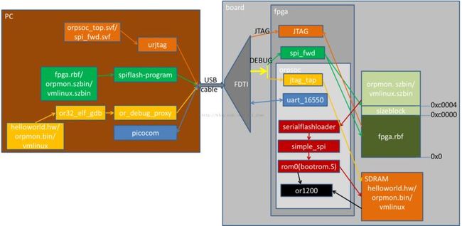
上面说了ORPSoC复位后的操作,但是在复位之前呢,如下图:
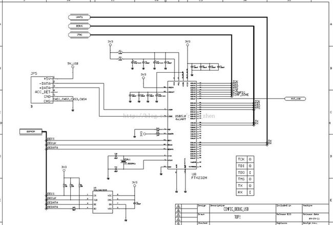
上面的机制可以通过schematic来进一步验证:
说明:
1》我们之前的实验都是通过jtag工具将svf文件,经FPGA本身的JTAG模块将ORPSoC配置到FPGA,然后通过or32-elf-gdb工具将可执行bin文件,经ORPSoC中的jtag_tap模块load到SDRAM中,再通过spr npc 0x100,设置启动地址,最终启动helloworld.HW ,orpmon和linux。最后通过picocom工具接受uart16550的内容,显示出来。
2》上面的过程,断电之后是不保存的,所以每次上电需要重新操作一遍才行。如果想上电自动执行,就需要将ORPSoC和需要执行的软件实现烧到外部的flash或者EEPROM或者SD card里面。
3》要想烧写外部的flash,首先需要将spi_fwd模块通过jtag工具将spoi_fwd.svf配置到FPGA里面,然后通关过spiflash-program工具将对应的rbf文件(ORPSoC的fpga bit文件),将orpmon.sizebin(前4字节是文件大小)/vmlinux.sizebin烧到0xc0000地址。这样上电之后,FPGA自动配置ORPSoC,然后or1200通过rom0中的bootrom.S经simple-spi模块和serialflashloader模块将flash中的软件copy到SDRAM,并运行之。
注:
1》spi_fwd和jtag_tap两个模块都是用户逻辑,并且两个模块对应的FPGA的引脚是一样的,两个模块对应的驱动工具分别是spiflash-program和or32-debug-proxy。ubuntu本地和官网svn有对应的c语言source code。感兴趣的可以下载下来看一下。
2》一般综合ORPSoC的工程后会自动生成rbf文件如果不能生成,需要手动生成,具体操作步骤,请参考后面的附录。
3>数据流向,从SD card启动。
上面分析了从外部flash启动的数据流向路径,要想从SDcard启动怎么办呢?步骤如下:
1》rbf文件仍然需要烧到外部的flash。这样上电之后FPGA本身的config模块才会自动load rbf文件内容来实现配置FPGA。
2》将软件事先通过PC烧到SDcard里面(起始地址要记住)。
3》修改bootrom.S代码,实现SD card controller的驱动,并将软件从SDcard copy到SDRAM。
2,program spi flash
步骤如下:
1>配置spi_fwd模块到FPGA芯片
$ cd ~/program-spi-flash
$ jtag ./program_spi.jtag
2>擦除flash
$ ./spiflash/spiflash-program -e
3>将ORPSoC的rbf文件烧到flash的0x0地址
$ ./spiflash/spiflash-program -p /home/openrisc/fpga_dev_board/ordb2a-ep4ce22/output_file.rbf
4>将booloader/vmlinux的sizebin文件烧到flash的0xc0000地址,具体烧什么要看你的板子的flash的大小而定(板子后面的U6和U7的型号),如果太小可以自己换一个大的(up to 8M bytes)。
$ ./spiflash/spiflash-program -a 0xc0000 -P /home/openrisc/program-spi-flash/vmlinux.sizebin
或者
$ ./spiflash/spiflash-program -a 0xc0000 -P /home/openrisc/program-spi-flash/orpmon.or32.sizebin
注:上面的2-4步可以通过一条命令实现:文件路径需要修改正确。
spiflash-program -e -p output_file.rbf -a 0xc0000 -P orpmon.or32.sizebin
5>重新插拔USB线
6>打开串口工具picocom
$ picocom --b 115200 --p n --d 8 --f xon /dev/ttyUSB2
7>应该能看到orpmon的输出信息,如下图(注:下图是我刚买回板子后用win7下的hyperterminal测试的截屏,不是这次实验的截屏。这次实验没有成功,原因还在查找中。)
附录A 生成rbf文件
如下图,根据sof文件生成rbf文件:用quartus_cpf工具生成。如果连sof文件都没有,可以用programmer工具根据svf文件生成sof文件。
附录B ORPSoC运行软件实验参考文档
===========================================================
Running Software on Hardware
===========================================================

This FPGA development board has been developed specifically
to fit a OpenRISC processor design, with the smallest form-factor
and lowest cost.

The board is called: ordb2a-ep4ce22 (OpenRisc Development Board 2A)

More detailed information can be found at the link below:
http://opencores.org/or1k/ordb2a-ep4ce22


===========================================================
Connecting ORSoC's OpenRISC-FPGA-development-board
===========================================================

1. Connect your ordb2a-board to your computer using the
   USB connector located on the top-left corner on the board.

2. The FPGA is programmed with a pre-compiled OpenRISC
   processor SOC-design, with Ethernet, SDHC, UART and
   SDRAM support. And with a small boot-loader (orpmon) that is
   stored in the external SPI-flash. The boot-loader should
   now be loaded and executing by the OpenRISC processor.

3. Open up a new terminal and type:
   $ picocom --b 115200 --p n --d 8 --f xon /dev/ttyUSB2

   Press "Enter" and you should now see a print-out in your
   terminal-window showing: ORSoC devboard>

   You now have a command-prompt "ORSoC devboard>" controlling
   the orpmon-software.
   By typing "help", all the diffent commands will be listed.
   For example you can start a coremark-test (cpu benchmark test),
   by typing "coremark 30"


===============================================================
Program ORSoC's OpenRISC-FPGA-development-board and run Linux
===============================================================

1. Connect your ordb2a-board to your computer using the
   USB connector located on the top-left corner on the board.

2. Start a terminal and type:
   $ cd ~/fpga_dev_board/ordb2a-ep4ce22
   $ jtag ./program_fpga.jtag

   The file "program_fpga.jtag" defines what FPGA programming file
   that should be used.

3. The FPGA is now programmed with a pre-compiled OpenRISC
   processor SOC-design, with the OpenRISC processor, Ethernet,
   SDHC, UART and SDRAM support. An small boot-loader is stored
   in the SPI-flash and should now be loaded and executed
   by the OpenRISC processor.

4. Let's now try and download Linux to the SDRAM and then boot it
   on the OpenRISC SoC design. There are many ways that we can
   boot Linux, we can use GDB, we can use orpmon and download it
   using TFTP, or we can program the SPI-flash. We will using GDB
   in demo. Open up a new terminal tab (shift+ctrl+t) and type:
   $ /opt/or_debug_proxy/bin/or_debug_proxy -r 55555

   This starts a program (or_debug_proxy) that controls the
   USB connection and communication between the GDB debugger and
   the OpenRISC processor.

   You should see the follwoing print-out:

   "
   Connecting to OR1k via USB debug cable
   Initialising USB JTAG interface
   JTAG ID = a188a928
   Stalling OR1K CPU0
   Read      npc = 0001727c ppc = 00017278 r1 = 00031774
   Waiting for gdb connection on localhost:55555
   Press CTRL+c to exit.
   "

5. Open up a new terminal tab (shift+ctrl+t) and type:
   $ picocom --b 115200 --p n --d 8 --f xon /dev/ttyUSB2

   This UART connection will be our Linux-terminal when we boot-up
   Linux on the OpenRISC SoC-design.


6. Open up a new terminal tab (shift+ctrl+t) and type:
   $ cd ~/soc-design/linux
   $ make ARCH=openrisc defconfig
   $ make ARCH=openrisc
   $ or32-elf-gdb

   The GDB-debugger is now started and you need to connect it to
   the or_debug_proxy program, by typing:
   (gdb) target remote :55555

   GDB is now connected to the OpenRISC processor and are now
   waiting. Lets now download the Linux-image, by typing:
   (gdb) file ./vmlinux
   Answer "y" on the questions.

   (gdb) load

   The actual download of the Linux image is now in progress and
   this takes some time, since the JTAG interface is not the
   fastest one. The following load information should appear:

   "
   Loading section .text, size 0x22bd34 lma 0x0
   Loading section .rodata, size 0x49860 lma 0x22c000
   Loading section __param, size 0x1c0 lma 0x275860
   Loading section .data, size 0x15760 lma 0x276000
   Loading section __ex_table, size 0xa50 lma 0x28b760
   Loading section .head.text, size 0x4000 lma 0x28e000
   Loading section .init.text, size 0x12348 lma 0x292000
   Loading section .init.data, size 0x155e54 lma 0x2a4360
   Start address 0xc0000000, load size 4160160
   Transfer rate: 86 KB/sec, 4015 bytes/write.
   "

   Now we want to set the program-counter to start executing
   from address 0x100, by typing:
   (gdb) spr npc 0x100

   Now let's boot up Linux on the FPGA development board, by typing:
   (gdb) c

   You should now see Linux booting in the picocom-terminal-window
   that was opened earlier. And you should get a prompt where you
   can play around with the Linux port that is running on the
   OpenRISC processor system.

   For example, you can plug in your board into your Ethernet network
   and get an IP address by typing:
   # ifup eth0

   Your network should now provide your board with an IP address (DHCP)
   and you can test your connection by pinging a known IP address.


====================================================================
Program ORSoC's OpenRISC-FPGA-development-board with bare-metal SW
====================================================================

1. Connect your ordb2a-board to your computer using the
   USB connector located on the top-left corner on the board.

2. Start a terminal and type:
   $ cd /home/openrisc
   $ jtag ./program_fpga.jtag

   The file "program_fpga.jtag" defines what FPGA programming file
   that should be used.

3. The FPGA is now programmed with a pre-compiled OpenRISC
   processor SOC-design, with Ethernet, SDHC, UART and
   SDRAM support. An small boot-loader is stored in the SPI-flash
   and should now be loaded and executed by the OpenRISC processor.

4. Let's now try and download a bare-metal application (hello world) to
   the board and run it. Open up a new terminal and type:
   $ /opt/or_debug_proxy/bin/or_debug_proxy -r 55555

   This starts a program (or_debug_proxy) that controls the
   USB connection and communication between the GDB debugger and
   the OpenRISC processor.

   You should see the following print-out:

   "
   Connecting to OR1k via USB debug cable
   Initialising USB JTAG interface
   JTAG ID = a188a928
   Stalling OR1K CPU0
   Read      npc = 0001727c ppc = 00017278 r1 = 00031774
   Waiting for gdb connection on localhost:55555
   Press CTRL+c to exit.
   "

5. Open up a new terminal and type:
   $ picocom --b 115200 --p n --d 8 --f xon /dev/ttyUSB2

   This UART connection will be a UART-terminal and will
   receive the Helloworld application's printf text.


6. Open up a new terminal and type:
   $ cd ~/soc-design/helloworld-or1ksim
   $ or32-elf-gdb

   The GDB debugger is now started and you need to connect it to
   the or_debug_proxy program, by typing:
   (gdb) target remote :55555

   GDB is now connected to the OpenRISC processor and are now
   waiting. Lets now download the Linux-image, by typing:
   (gdb) file ./helloworld_hw
   Answer "y" on the questions.

   (gdb) load

   The actual download of the Helloworld-image is now in progress and
   this takes some time, since the JTAG interface is not the
   fastest one. The following load-information should appear:

   "
   Loading section .vectors, size 0x2000 lma 0x0
   Loading section .init, size 0x28 lma 0x2000
   Loading section .text, size 0x494c lma 0x2028
   Loading section .fini, size 0x1c lma 0x6974
   Loading section .rodata, size 0x50 lma 0x6990
   Loading section .eh_frame, size 0x4 lma 0x69e0
   Loading section .ctors, size 0x8 lma 0x89e4
   Loading section .dtors, size 0x8 lma 0x89ec
   Loading section .jcr, size 0x4 lma 0x89f4
   Loading section .data, size 0x9b8 lma 0x89f8
   Start address 0x2028, load size 29616
   Transfer rate: 42 KB/sec, 1851 bytes/write.
   "

   Now we want to set the program-counter to start executing
   from address 0x100, by typing:
   (gdb) spr npc 0x100

   Now lets start the Helloworld_hw application on the FPGA
   development board, by typing:
   (gdb) c

   You should now see the follwoing printout in the
   picocom terminal window that was opened earlier:

   "
   Hello world!!!!
   "

   Now you can start developing your own
   bare-metal applications :-)


===========================================================
Programming external SPI-flash
===========================================================
The external SPI flash contains both the FPGA programming file
and a bootloader (orpmon).
Below are information on how to program the SPI with these two files:


   1. Download an FPGA-programming file that just connects the
      FTDI JTAG signals to the SPI flash IOs.
      $ cd ~/program-spi-flash
      $ jtag ./program_spi.jtag

   2. Erase the SPI flash before programming it:
      $ ./spiflash/spiflash-program -e


   3. Program the SPI flash with an FPGA programming file (rbf-format):
      $ ./spiflash/spiflash-program -p /home/openrisc/fpga_dev_board/ordb2a-ep4ce22/output_file.rbf

   4. Program the SPI-flash with OpenRISC SW application (select only one):

      4a. Program OpenRISC Linux (requires a large SPI flash):
          $ ./spiflash/spiflash-program -a 0xc0000 -P /home/openrisc/program-spi-flash/vmlinux.sizebin


      4b. Program OpenRISC bootloader (orpmon)
          $ ./spiflash/spiflash-program -a 0xc0000 -P /home/openrisc/program-spi-flash/orpmon.or32.sizebin


Unplug the board and connect it again to load the new flash contents.


Steps 2-4 can also be combined like so (directory paths omitted for brevity):
   spiflash-program -e -p output_file.rbf -a 0xc0000 -P orpmon.or32.sizebin

Sizebin files are produced from binary memory dumps using bin2binsizeword:
   ~/soc-design/orpsocv2/sw/utils/bin2binsizeword ~/soc-design/orpmon/orpmon.or32.bin ~/program-spi-flash/orpmon.or32.sizebin


Good luck and welcome to the OpenCores OpenRISC community ;-)


Delivered by: [email protected], [email protected]
2011-12-15
3,小结
本小节介绍了ORPSoC的系统setup过程,并尝试烧写外部的flash,但是没有成功,如果有哪位读者做过类似的工作,或者有什么意见和建议,可以写评论。
thanks in advance!


