Reverse engineering NAND Flash for fun and profit
Reverse engineering NAND Flash for fun and profit
Flash memory is used everywhere. It is in the game console in your living room; it is in the phone in your pocket; it is in the router in your network. Flash memory was invented by a Japanese researcher, Dr. Fujio Masuoka around 1980 and it is so amazing that this technology is now used everywhere - more than 30 years after its invention.
A few weeks ago, I had the chance to reverse-engineer a hardware device we bought from eBay. The purpose of our investigation was to penetration-test the device, but I had no idea how to approach it. I was locked out of the machine by a password and even the seller didn’t know what it was (I assumed the seller was just a sort of liquidation company). However, the machine was so cheap that we couldn’t complain about the deal – password or not. So to penetration-test this machine, we knew there’d have to be some level of hardware reverse engineering.
When we opened up the machine, we found that it was using an ARM CPU (Samsung S3C2410AL) and had chips related to communications through Ethernet and serial ports. We also found that it had two DRAM (Dynamic Random Access Memory) chips and one Flash memory chip (Samsung K4S561632H). (I think this is a pretty typical setup for modern embedded machines.) First, we tried looking for JTAG ports, but got kind of stuck with that for some reason. Then we thought we might try dumping Flash memory directly.
De-soldering
The first step was taking out the Flash memory chip itself. I had read about some approaches that connect wires to a chip directly without extracting it. There’s even a clip-type socket that you can put over a Flash memory chip directly without taking it out. We tried that approach, but the problem was that when you supply electricity to the Flash memory, it actually flows through other parts of the board and wakes up other chips and it interferes with our bit-banging operation. So we decided to extract the chip. This might sound a little tricky, but it‘s a well-established process. You can get products that you apply to the pins on the chip to melt out the existing solder, but while this approach is valid, we decided to use a hot air gun to heat up the solder and take the chips out while the solder was fluid. It took us about 30 seconds to 1 minute to take the Flash memory out.
Figure 1 De-soldering in progress with hot air gun
Figure 1 shows the process of blowing hot air to melt the solder, while Figure 2 shows the extracted Flash memory chip. Just be sure to not touch the pins as they are really sensitive. If those pins are not aligned, you might have a hard time trying to make things work correctly.
Figure 2 Extracted NAND Flash
Bit-banging
We searched for information about Flash memory dumping and found many different approaches. The approach we thought the most useful and decided to try was FT2232H bit-banging. Bit-banging is a method of controlling chips directly from software through serial communication. FT2232H NAND flash reader had some good information on the steps to take and the author had also released some basic schematics and toolsets. This method uses the FT2232H chipset, which converts USB to serial protocol, to send control commands to NAND Flash directly. The software library the author used was libFTDI, which supports various FTDI chipsets. One good thing about using this library is that it supports multiple OSes including Linux, Windows, MacOS X. While the author released software that can use this library to control Flash memory, another project that had forked out from the original code caught our eye. The new forked project supports writing to NAND flash as well as reading from it and we found this new code to be more stable (even just for the reading operations).
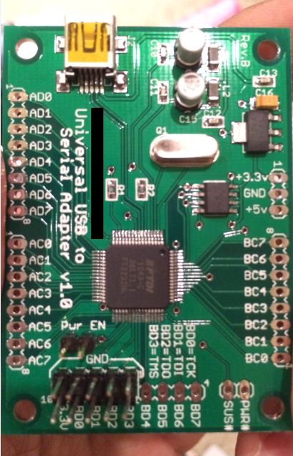
Instead of soldering the chip onto a new breakout board, we bought a ready-made breakout board for the FTDI chipset (Figure 3). There are quite a few variants of FTDI breakout board on the market, and as this FTDI chipset is quite popular with hobbyists, it shouldn’t be difficult to find something similar.
Figure 3 FTDI breakout board
As the NAND Flash memory we were trying to dump was 48 pin, we purchased a TSOP48-to-DIP48 converter for easy wiring. Figure 4 shows the final device we came up with. We just loaded the extracted Flash memory chip on the TSOP48 socket and connected the device to the laptop using a USB cable.
Figure 4 Bit-banging in action
Pages, blocks, ECC
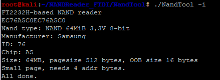
Figure 5 shows the basic information identified by NandTool. It is a 64MB Flash memory with a page size of 512 bytes. OOB size is 16 bytes. This information is valuable as the dumped out image uses it for post-processing.
Figure 5 NAND Flash Information
In NAND Flash memory, a page is the minimum element for data storage. A page in NAND Flash memory is a similar concept to a sector on a hard disk. 32 pages make one block in our case. The thing here is that there can always be physically damaged blocks or pages. The OOB area is used to store this out of band information. The actual usage of the OOB area differs slightly between vendors and chip models. Even the method for locating the OOB area is variable.
Figure 6 Data & OOB Area
We found that the first 3 bytes of the OOB area is used for ECC (Error Correcting Code). ECC uses the concept of Hamming code, to correct 1 bit errors from the page data. The concept is very similar to parity bit, but this checksum can also be used for correcting a single corrupt bit (rather than just detecting the error). This is useful not only for ensuring data integrity, but also self correcting when the error is minor. Hamming code itself was invented in 1950 and it is still used in many areas. The amazing thing is that you need just 3 bytes to cover 512 bytes of data. The problem here is that each vendor uses a slightly different algorithm. You just need to figure out what algorithm it uses to make sure every page is intact. There are some popular known algorithms used by each vendor and you need to tweak those if the known algorithm doesn’t work. Figuring out the ECC algorithm is really important because when you want to modify the data on the memory chip, you need to re-calculate the ECC. Also, you need to check if there are any bad blocks in the memory image. Each chip has a slightly different approach for that and you need to figure that out too.
Memory layout
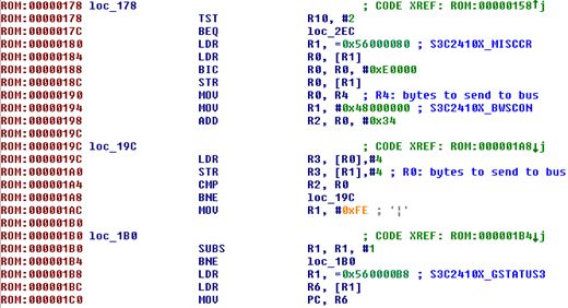
So after figuring out how the lowest level page system works, you need to extract pages from the original dump. After that, you are ready to work on the layout. Based on the configuration, the CPU tries to load the bootloader from different devices. If Flash memory exists, the CPU usually tries to load instructions from the first page of the Flash memory . This is usually called the “1st stage bootloader”. You can see our example in Figure 7. It performs very low level operations to initialize values for the CPU. After that it jumps to the 2nd stage bootloader.
Figure 7 1st stage bootloader
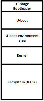
Actually, U-boot was used as the 2nd stage bootloader in our case, which is typical with embedded systems. Figure 8 shows the typical Flash memory layout in embedded systems in general. U-boot loads the OS kernel and the kernel mounts the file system. We found that our target system was using the Linux kernel and JFFS2 type file system. This is also very typical. Now, after we figured out the memory layout, we needed to dig into whatever we wanted to acquire. In this case, we wanted to access the file system.
Figure 8 Flash memory layout
Mounting the file system
The good news is that you can use a Linux system to load a JFFS2 image file. You just need to use the mtdram feature. To initialize the mtdram feature, run the commands shown in Figure 9.
Figure 9 Loading required modules
After extracting the jffs2 part from the Flash image file, use the “dd” command to write the bits to the mtdblock device as shown in Figure 10. After that you can mount that mtdblock to whatever location you want.
Figure 10 Mouting through mtdblock
If you go to the mounted directory, you will see the files you wanted to grab (Figure 11).
Figure 11 Mouting extracted JFFS2 data
Now that you have everything you wanted, you can dig into the target files using IDA. There may be a lot of interesting things to be found. Of course, that means it’s time to hang up your hardware reverse engineering hat and let your software reverse engineering skills take the lead.


