ATI图形芯片ABC
http://www.botchco.com/agd5f/?p=51
作者agd5f是开源linux AMD/ATI显卡驱动(radeon)的主要维护者.显卡最重要的两个功能:渲染(render)和显示(display),关于渲染的资料和讨论已经很多了,但很少有关于display的一个系统的介绍.intel和amd都相继开放了一些programming document出来,对于render部分的2D/3D/Video等graphics core,除了寄存器spec以外还有较详细的内部架构方面的文档,对理解其芯片工作原理帮助很大;但描述display hardware的文档就只有生涩的寄存器spec了,缺乏一个类似overview的架构的介绍.读这些硬生生描述display hardware寄存器的陈列,只能说看着是一头雾水.这篇精彩博文算是一个不错的补充吧:
Notes about radeon display hardware
Display routing can be confusing so here are the basics. The simplified route from framebuffer to monitor looks like this:
framebuffer -> crtc -> encoder -> transmitter -> connector -> monitor
The framebuffer is just a buffer vram that has an image encoded in it as an array of pixels.
(framebuffer翻译过来叫'帧缓冲区',通俗点可以叫'显存'.该buffer的每个存储单元存放的对象是'像素'.图形处理芯片的另一个功能:渲染'render hardware',负责在'显存'中产生像素.而display hardware则负责把framebuffer中的像素'发射'到crt,lcd等device上)
The crtc reads the data out of the framebuffer and generates the video mode timing in conjunction with a PLL. The crtc also determines what part of the framebuffer is read; e.g., when multi-head is enabled, each crtc scans out of a different part of vram; in clone mode, each crtc scans out of the same part of vram.
(framebuffer的像素被CRT Controller,又叫crtc按照一定的时序一行一行地scan out.crtc还可以控制需要scan的区域.framebuffer如果是一张纸,那么crtc可以起到viewport的功能,只裁剪出一个矩形区域出来让你看.除了scan out像素以外,crtc还负责输出一些monitor需要的时序同步信号,典型的如vsync和hsync,即场同步和行同步信号.这两个基本的同步信号用来通知显示设备什么时候一个新的扫描行开始了和一个新的图像帧开始了.对于一些设备如CRT来说,这就意味着要移动电子枪了)
The encoder takes the digital bitstream from the crtc and converts it to the appropriate format for the requested output.
The transmitter takes the digital representation and converts that to the appropriate analog levels for transmission across the connector to the monitor.
(crtc读取framebuffer后输出的信号一般有像素数据值,同步信号hsync和vsync,以及pixel clock,这些信号一般 都是适合计算机处理的并行TTL数字信号. 比如真彩色的像素格式RGB888,每个color component都是8位,即需要8根数据线.这自然是不适合于在显示设备之间进行传输的.于是,crtc输出的信号需要编码到一种适合传输的信号流.
比如CRT,接口里传输颜色的只有R、G、B三根数据线,其上承载的信号电压值表达了要传输的symbol value.即,crtc输出的TTL数字信号被D/A Convertor编码成了模拟信号,如下图.这个D/A Convertor就是编码器.

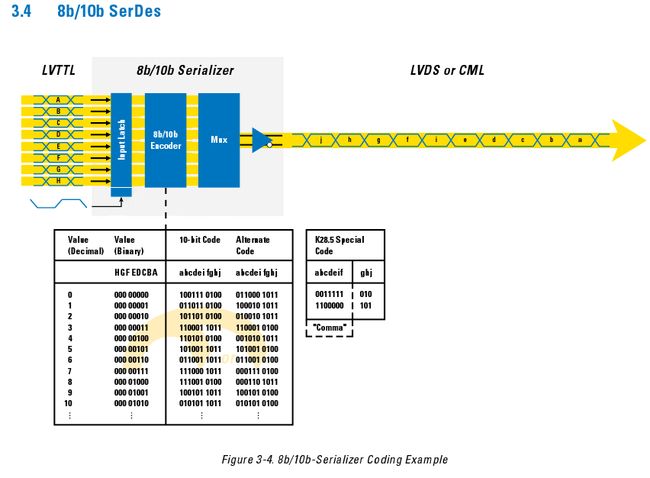
又如LCD(笔记本上的flat panel)的数字接口标准之一LVDS.虽然传输的不是模拟信号,但也是采用串行链路.所以就需要有一个编码器能对输入的并行的crtc比特流做串行化操作,这一般简称SerDes.从LVDS的WIKI可知,LVDS是物理层的标准,它并不对其应用强加bit encoding的模式,除了采用8 bit (像素格式为RGB888的一个color component就是8位) 的串行编码外,也可以采用8b/10b等encoding,这是一种将并行的8位数字信号变成串行的10位数字信号的编码方式,主要为了DC Banlance.
Encoder负责改变symbol value的表达方式,transmiter则该改变物理的信号形式.如LVDS transimiter就要把TTL信号转变为差分信号.DAC transmitter将数字的转变为模拟的.对于LVDS和TMDS等标准来说,它们其实都只定义了物理层的协议即transmitter该干什么,没有为encoder作什么强加限制,显示设备的设计者可以在有限的几种串行编码中自行选择.)
The connector provides the appropriate plug for the monitor to connect to.
(connector也叫port,是最终device如crt、lcd可插接的物理接口.它本身不会去调理信号,只是作为一个信号输出的端口,以致可以承载负载.一块板子(card)有多少connector,以及支持什么connector都是由Oem厂商根据图形芯片的encoder/transmitter的信号输出能力来决定,一般我们之所以说这款显卡支持多少路hdmi输出,支持多少路tv输出,最终都是由它来决定.)
Radeon Hardware:
On older asics (radeon (r1xx-r4xx), DCE 1.x (r5xx) and DCE 2.x (early R6xx/RS600/RS690/RS740)) the encoders and transmitters
tended to be one combined block that supported a single output type; e.g., a TMDS/HDMI block or an LVDS block. The DCE1.x/2.x LVTMA block was kind of an exception in that it could support both TMDS and LVDS signaling, but the encoder part and the transmitter part were not routeable. The LVTMA encoder was hardwired to the LVTMA transmitter; the TMDSA encoder was hardwired to the TMDSA transmitter, etc. Analog outputs (DACs) are also generally one block rather than being split into a separate routeable encoder and transmitter since there are fewer types of analog outputs (pretty much just TV and VGA). The digital outputs were split into separate encoders and transmitters because there are lots of different types of digital outputs required for systems (HDMI, DP, DVI, LVDS, eDP, etc.).
(radeon芯片采用了'分离式'的encoder和transimitter的设计.不过文中提到的unroutable的分离式我认为其实就是相当于没分离.分离式的encoder和transmitter有什么好处呢?像LVDS和TMDS标准,在物理层的信号调理是不一样的,但是他们的编码方式却可能一样.那么对于chipmaker,当然是希望芯片有够flexibility,这样OEM厂商能在card上订制丰富的connector如HDMI,DP,DVI,LVDS等,最好一块板子都带上,用户想怎么接就怎么接.但是有多少个connector就需要多少个tranismiiter,试想把一个transimitter和几个connector耦合会发生什么情况?transimitter该工作在什么模式下?所以,如果是将tranismitter和encoder绑定在一起,势必造成浪费,毕竟有一些encoder输出的其实是相同的编码,这些浪费的encoder自然会增大芯片的面积,产生多余的热量.假设encoder可以更general,更abstract一些,只有两种区别:DAC和DIG,分别驱动模拟的transmitter和数字的transmitter,不管transmitter是什么display standard,那么这两种encoder各自只需要一个就够了.不过这是当crtc也只有一个的时候,如果crtc有两个,那么只有一个encoder是不够的,前面说过crtc可以scan framebuffer的一个指定区域,当两个crtc scan的区域不一样时,自然输出的timing signal也是不一样的,所以至少要两个或两对encoder才能满足要求.)
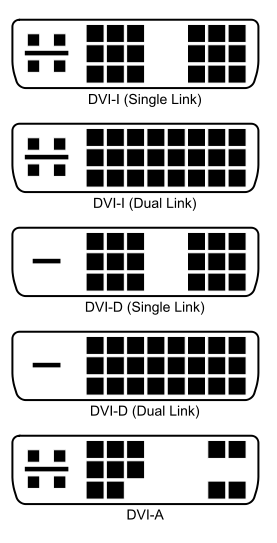
The links (A,B,A+B) are required for things like dual link DVI or LVDS, where one link doesn’t provide enough for a particular mode. In that case, two links are used rather than one to transmit the data to the monitor( 从 WIKI知道,dual link一般是为了能支持更大的显示模式,采取的一种能提高显卡到设备之间的bandwidth的方式.一条link可以看成是一路color data传输的通路,比如上面提到的LVDS,3对差分信号线用于传输一个像素,那么dual link就是再增加3对差分信号线,总共6对,一个pixel colock就可以传输2个像素,下图可以看到dual link DVI比single link DVI的connector多了1/3的output pin) .
The LVTMA block on DCE3.0 was basically a UNIPHY block that also supported LVDS; DCE3.0 UNIPHY only supported TMDS/HDMI/DP. On DCE3.2, all the UNIPHY blocks supported all output types (LVDS/TMDS/HDMI/DP/etc.), so there was no need to make a distinction.
(前面说在DCE 1.x/2.x上,有一个可以既工作在LVDS模式下,又可以工作在TMDS模式下的transimitter叫LVTMA,很强大.到了DCE3.x,更狠的UNIPHY来了,UNIPHY就像一个general purpose的transimitter,所有主流的数字显示标准基本上都支持.强大的硬件自然需要智能的软件来配合,驱动程序这时就要负责根据实际情况来设置UNIPHY connector到底工作在何种模式下.)
One or more transmitters are wired to a connector. Having support for six transmitters means we can support up to six digital connectors (three transmitters (UNIPHY0/1/2, two links each (A,B)). So physically your system might look like:
1. DACB + UNIPHY0 links A,B -> dual link DVI-I port
2. UNIPHY1 link B -> single link DVI-D port
3. UNIPHY1 link A -> HDMI type A port
4. UNIPHY2 link A -> single link LVDS port
5. DACB -> TV port
6. DACA -> VGA port
You need to drive those connectors with timing (crtc), and the proper digital or analog data stream encoding (DIG encoder or DAC), and
appropriate transmission levels (UNIPHY/LVTMA/DAC). So the logical path would look like:
timing -> encoder -> transmitter -> connector
So for example 2 above the path might look like:
crtc 0 -> DIG1 -> UNIPHY1 link B -> single link DVI-D port
And example 4 might look like:
crtc 0 -> DIG2 -> UNIPHY2 link A -> LVDS port
And example 6 might looks like:
crtc 1 -> DACA -> DACA -> VGA port
(既然ATI提供这么牛X的chip,上面有支持几乎所有display standard的transmitter,oem厂商不用岂不浪费?3 transmitter和2 links可以提供最多6种组合,oem厂商在板子上怎么选择是oem自己的事情,那么A的板子上有一个DP和一个CRT,B的上面有一个DVI,一个HDMI和一个CRT,其transmitter的设置都不一样的,signal routing也不一样,radeon driver总不能为每个oem厂商都订制一份driver吧。但是,oem是可以订制bios的,所以,driver就可以从bios中知道这么一张signal routing的table,根据这张table,register setting就搞定了)
Until evergreen, radeon chips only supported two crtcs, so there were only two encoder blocks. With evergreen, there are six crtcs, so there are also have six digital encoder blocks since you might want to run six independent displays. In a way evergreen has gone back to being more like the earlier DCE 1.x/2.x designs in that the encoders are not individually routeable anymore; they are hardwired to a particular transmitter. E.g., on evergreen DIG0/1 are hardcoded to UNIPHY0. There are two encoders since UNIPHY links A and B can be used independently or combined (for dual link). In the combined case, you’d only use one encoder, but it would drive both links. On DCE3.x, the encoders and transmitters are separately routeable since you have more transmitters (three transmitters, six possible links) than encoders (two) and you need to be able to drive different combinations.
Evergreen Hardware:
The number of active heads supported depends what connectors the OEMs put on their boards. Generally, most seem to be one DP and several non-DP outputs for a total of three possible independent screens, but you could in theory design a board with more two or more DP outputs and some combination of non-DP ports for between two and six independent screens. However, as you add more possible simultaneous screens, you need more memory bandwidth, so that needs to be taken into account when designing the board. A lot of current boards have two dual-link DVI ports, an HDMI port, and a DP port. That combination uses all the possible encoders/transmitters, so you’d have to give up one of those to add another DP port.
The evergreen hardware has two PLLs, six crtcs, two DACs, and six digital encoders/transmitters (which can be used for LVDS/TMDS/DP/eDP/HDMI). DP runs at a fixed clock, so you don’t need a separate programmable PLL for it. That gives you some combination of up to two non-DP outputs, and up to six DP outputs for a maximum of six possible independent screens. Dual-link DVI ports require two digital transmitters (one for each link), so a dual-link DVI port would use two of the six possible transmitters, leaving four for other digital outputs. Two dual-link DVI ports would use four digital transmitters which would leave two for other digital outputs. DP only requires 1 transmitter. So in order to use a dual-link DVI monitor on a DP port, you need an active converter since native dual-link is not possible due to the lack of a second transmitter when running in DVI pass-through mode. You can use a passive DP->DVI converter on any DP port; all of the DP ports support pass-through and can be configured for HDMI or DVI. However, you are limited to two active non-DP monitors (due to there only being two PLLs) at a time. Also the monitors being used for pass-through (passive converter) have to be single link DVI since DP only has one digital transmitter connected to it. For more than 2 non-DP monitors, or dual-link DVI, you will need an active converter.