flash memory技术
Toshiba
developed flash memory from
EEPROM
(electrically erasable programmable read-only memory) in the early 1980s and introduced it to the market in 1984. The two main types of flash memory are named after the
NAND
and
NOR
logic gates
.
Although flash memory is technically a type of EEPROM, the term "EEPROM" is generally used to refer specifically to non-flash EEPROM which is erasable in small blocks, typically bytes.
[ citation needed
]
Because erase cycles are slow, the large block sizes used in flash memory erasing give it a significant speed advantage over non-flash EEPROM when writing large amounts of data. As of 2013, flash memory costs much less than byte-programmable EEPROM and had become the dominant memory type wherever a system required a significant amount of non-volatile
solid-state storage
.
Floating-gate transistor
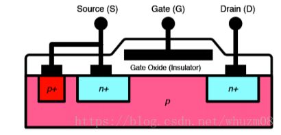
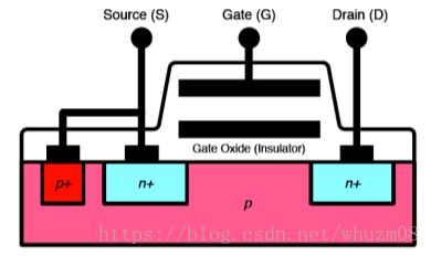
In flash memory, each memory cell resembles a standard
MOSFET
except that the transistor has two gates instead of one.
Applying a gate-to-source voltage generates an electric field through insulator and creates a conduction channel through which current can pass from drain to source.
因为control gate和float gate之间是绝缘体,而float gate和
衬底之间是Gate
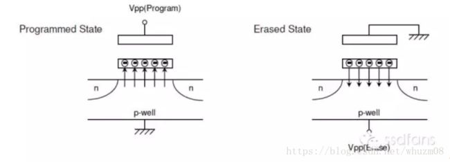
oxide,在强电场情况下还是会有电子被激活,打破束缚,这种方式称为tunnel效应,或者高速电子(又称为热电子)穿过Gate oxide进入FG,这种方式称为Channel Hot Electron injection。
Electrons residing on the floating gate remain there when power is removed。
写操作是将电子放置在FG上。擦除操作正好相反,是把电子从FG中吸出来。如下图所示:
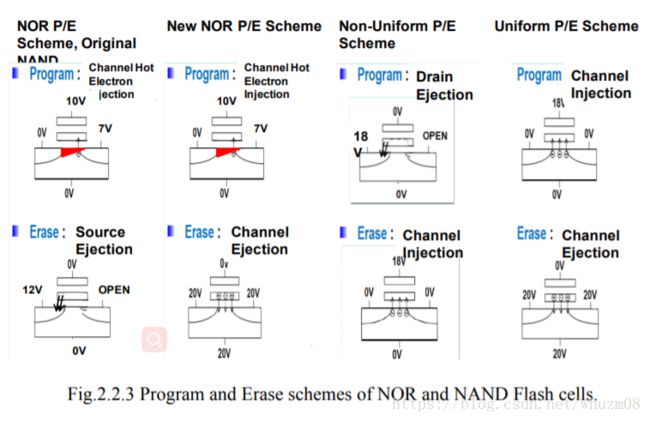
在FG上放置电子叫做injection,将FG上的电子排出叫ejection,主要有两种技术:
Channel Hot Electron injection (CHE) and Fowler-Nordheim (FN) channel injection
一旦FG放置了电子,当在CG上施加正电压时,它部分取消了加在CG上电压带来的电场影响,这样晶体管导通需要在CG上放置更高的电压,假如在FG上没有电子时,CG上放置电压Vt1时导通,在FG上放置电子后,CG上需要放置电压Vt2导通,满足Vt2 > Vt1
为了读出cell的值,在CG上放置一个电压V,要求Vt1
如果晶体管导通(代表数值1),那么FG上肯定没有电子
如果晶体管不导通(代表数值0),那么FG上肯定放置有电子
一个存储单元存储
1bit
数据的
NAND FLASH
,我们叫它为
SLC (Single Level Cell)
,
2bit
为
MLC (Multiple Level Cell)
,
3bit
为
TLC (Triple Level Cell)
。
对
SLC
来说,一个存储单元存储两种状态,浮栅极里面有无电子,读出数值就是电流导通与不导通两种状态
对
MLC
来说,一个存储单元存储四个状态,一个存储单元可以存储
2bit
的数据。通俗来说就是把浮栅极里面的电子个数进行一个划分,比如低于
10
个电子,判为
0
;
11-20
个电子,判为
1
;
21-30
,判为
2
;多于
30
个电子,判为
3, 读出数值就是电流的大小。
依次类推
TLC
,它的一个存储单元有
8
个状态,可以存储
3bit
的数据,它在
MLC
的基础上对浮栅极里面的电子数又进一步进行了划分,读出数值就是电流的大小。
同样面积的一个存储单元,
SLC
,
MLC
和
TLC
,依次可以存储
1,2,3bit
的数据,所以在同样面积的
LUN
上,
NAND FLASH
容量依次变大。
NOR flash
Intel Corporation
introduced the first commercial NOR type flash chip in 1988. [8]
NOR-based flash has long erase and write times, but provides full address and data buses, allowing
random access
to any memory location.
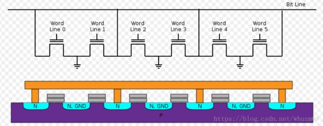
In NOR flash, each cell has one end connected directly to ground, and the other end connected directly to a bit line. This arrangement is called "NOR flash" because it acts like a
NOR gate:
when one of the word lines (connected to the cell's CG) is brought high, the corresponding storage transistor acts to pull the output bit line low.
在读取数据时,只在选中的word line上施加电压,其他的word line上均不加电压,这样如果bit line被拉低就说明导通了。
Reading from NOR flash is similar to reading from random-access memory, provided the address and data bus are mapped correctly. Because of this, most microprocessors can use NOR flash memory as
execute in place
(XIP) memory, meaning that programs stored in NOR flash can be executed directly from the NOR flash without needing to be copied into RAM first. NOR flash may be programmed in a random-access manner similar to reading. Programming changes bits from a logical one to a zero. Bits that are already zero are left unchanged. Erasure must happen a block at a time, and resets all the bits in the erased block back to one. Typical block sizes are 64, 128, or 256 KiB
.
To avoid needing unique driver software for every device made, special
Common Flash Memory Interface
(CFI) commands allow the device to identify itself and its critical operating parameters.
NAND flash
NAND flash architecture was introduced by Toshiba in 1989.
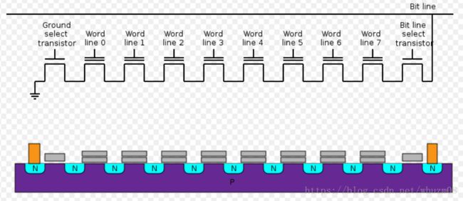
NAND flash also uses
floating-gate transistors
, but they are connected in a way that resembles a
NAND gate
: several transistors are connected in series, and the bit line is pulled low only if all the word lines are pulled high (above the transistors' V
T
). These groups are then connected via some additional transistors to a NOR-style bit line array in the same way that single transistors are linked in NOR flash.
在读出数据时,选中的word line上施加
Vt1
Despite the additional transistors, the reduction in ground wires and bit lines allows a denser layout and greater storage capacity per chip. (The ground wires and bit lines are actually much wider than the lines in the diagrams.) In addition, NAND flash is typically permitted to contain a certain number of faults (NOR flash, as is used for a
BIOS
ROM, is expected to be fault-free). Manufacturers try to maximize the amount of usable storage by shrinking the size of the transistors.
While reading and programming is performed on a page basis, erasure can only be performed on a block basis
NAND FLASH
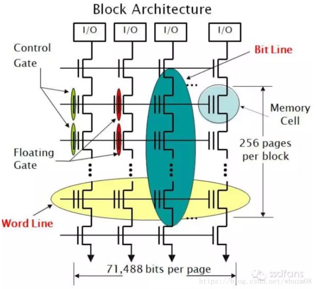
就是由成千上万这样的存储单元按照一定的组织结构组成的。
一个
WordLine
对应着一个或若干个
Page
,取决于
SLC,MLC
或者
TLC
。对
SLC
来说,一个
WordLine
对应一个
Page
;
MLC
则对应
2
个
Page
,这两个
Page
是一对:
Lower Page
和
Upper Page
;
TLC
对应
3
个
Page
。一个
Page
有多大,那么
WordLine
上面就有多少个存储单元(
Cell
),就有多少个
Bitline
。一个
Block
当中的所有这些存储单元(
Cell
)都是共用一个衬底的。
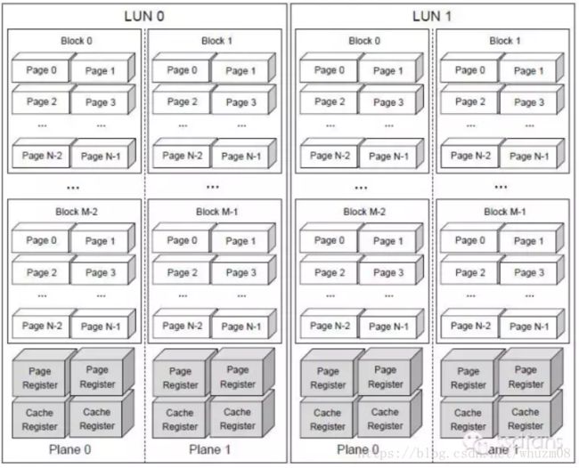
一个
NAND FLASH
内部存储组织结构是这样的:一个
Device
有若干个
DIE
(或者叫
LUN
),每个
DIE
有若干个
Plane
,每个
Plane
有若干个
Block
,每个
Block
有若干个
Page
。每个
Page
对应着一个
Wordline
,由成千上万个存储单元构成。
DIE/LUN
是接收和执行
FLASH
命令的基本单元。上图中,
LUN0
和
LUN1
可以同时接收和执行不同的命令。但在一个
LUN
当中,一次只能执行一个命令,你不能对其中的某个
Page
写的同时,又对其他
Page
进行读访问。
一个LUN又分为若干个Plane,一般为1个或者2个,现在也有4个Plane的NAND了。每个Plane都有自己独立的Cache Register或者 Page Register,一般情况下,两个Register内容都是一样的,其大小等于一个Page的大小。Host在写某个Page的时候,它是先把数据从Host传输到该Page所对应Plane的Cache Register当中,然后再把整个Cache Register当中的数据写到NAND FLASH阵列;读的时候类似,它先把这个Page的数据从FLASH阵列读取到Page Register,然后再按需传给host。这里按需是什么意思?就是我们读取数据的时候,没有必要把整个Page的数据都传出来给Host,按需选择数据传输。但要记住,无论是从FLASH 阵列读数据到Page Register,还是把Page Register的数据写入FLASH阵列,都是以Page为单位!
A group called the Open NAND Flash Interface Working Group (ONFI) has developed a standardized low-level interface for NAND flash chips. This allows interoperability between conforming NAND devices from different vendors. The ONFI specification version 1.0[44] was released on 28 December 2006. It specifies:
-
a standard physical interface (pinout) for NAND flash in TSOP-48, WSOP-48, LGA-52, and BGA-63 packages
- a standard command set for reading, writing, and erasing NAND flash chips
-
a mechanism for self-identification (comparable to the serial presence detection feature of SDRAM memory modules)
读操作:
A page corresponds to a row of cells and is accessed by a single wordline. VpassR (~6V) is applied to unselected wordline to be as a pass transistor.
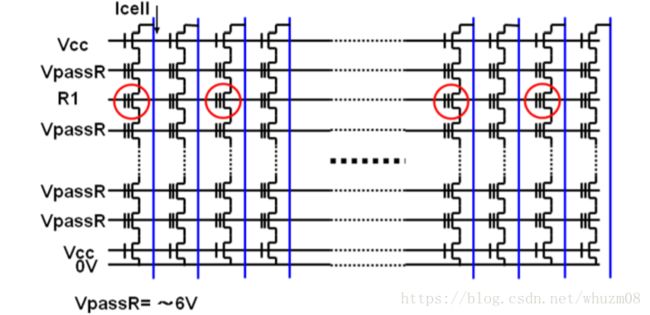
如果导通,相应的bit line为低,否则bit line为高
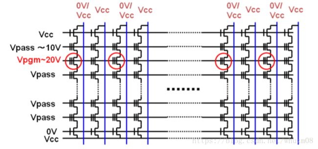
写操作:
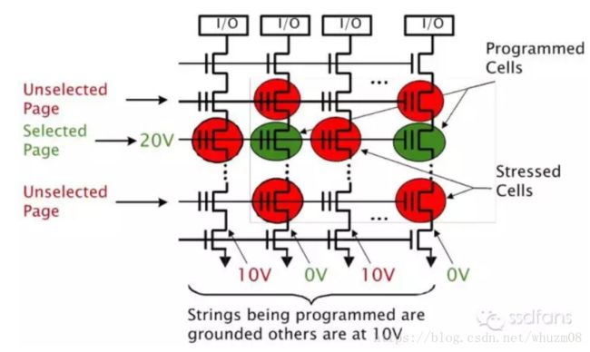
根据写入的数据控制bit line上的电压,如果写入0,则相应的bit line直接接地,这时在CG和D/S之间电压差20V,形成强电场,在tunnel效应下,电子进入FG,如果写入1,则相应的bit line上加10v电压,这时在CG和D/S之间电压差20V,电场不是很强,电子不能进入FG。
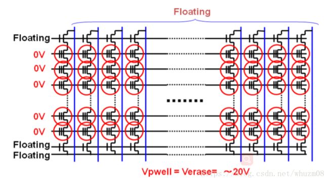
擦除操作:
nand flash的一些特点:
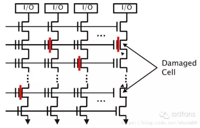
1.在
NAND
当中的存储单元中,先天就有一些是坏掉的,或者说不稳定的。并且随着
NAND
的不断使用,坏的存储单元越来越多
oxide layer被不可恢复的击穿变成了导体,因此FG不再能束缚电子
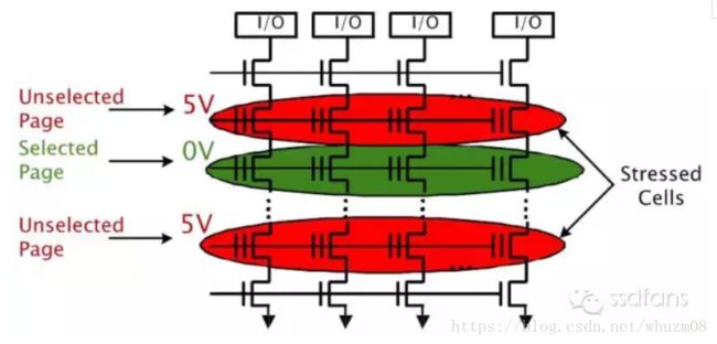
2. 读干扰(Read Disturb)。什么意思?从NAND读取原理来看,当你读取一个Page的时候,Block当中未被选取的Page控制极都会加一个正电压,以保证未被选中的MOS管是导通的。这样问题就来了,频繁的在一个MOS管控制极加正电压,就可能导致电子被吸进浮栅极,形成轻微的Program。从而最终导致比特翻转。但是,这个不是永久性损伤,重新擦除Block还能正常使用。注意的是,Read Disturb影响的是同一个Block中的其它Page,而非读取的Page本身。
3.
写干扰(
Program Disturb
)
。除了Read Disturb
会导致比特翻转,
Program Disturb
也会导致比特翻转。还是要回到
FLASH
内部的
Program
原理上来。
由于对擦除过的Block,其所有的存储单元初始值就 是1,所以Program的时候,只有写0的时候才真正需要Program。如上图所示,绿色的Cell是写0,需要Program的,红色的代表写1,并不需要Program。我们这里把绿色的Cell称之为Programmed Cells,红色的Cell叫Stressed Cells。写某个Page的时候,我们是在其 WordLine的控制极加一个正电压(上图是20V),对于Programmed Cells所在的String,它是接地的,不需要Program Cell所在的String,它是接一正电压(上图为10V)。这样最终产生的后果是,Stressed Cell也会被轻微Program。与Read Disturb不同的是,Program Disturb 影响的不仅是同一个Block当中的其它Page,自身Page也受影响。相同的是,都是不期望的轻微 Program导致比特翻转,都非永久性损伤,经擦除后,Block还能再次使用。
4. 电荷泄漏
存储在NAND FLASH存储单元的电荷,如果长期不使用,会发生电荷泄漏。不过这个时间比较长,一般十年左右。同样是非永久性损伤,擦除后Block还能使用。
ECC
An Error correcting code (ECC) is redundant data added to the original data. In event of errors, the combined data allows the recovery of the original data. The number of errors that can be recovered depends on the algorithm used.
The various algorithms used in ECC hardware are:
1. Hamming: For 1 bit
2.
Reed Solomon: For up to 4 bits of
3.
BCH : For more than 4 bits
Data stored in NANDs can get corrupted (randomly). There is an upper limit on the number of error per byte depending on the NAND process and the technology. SLC NANDs have less ECC requirements than MLC NANDs. The NAND datasheet gives the ECC requirement for the NAND device. For SLC NANDs, 1/4bits per 512 bytes are common currently. For MLC, devices with 4/8/16 bits per 512 bytes ECC requirements are in the market.
Assuming software ECC and enough spare bytes, any ECC algorithm can be used. The NAND device is oblivious to the ECC algorithm used to correct bit errors.
参考资料:
https://en.wikipedia.org/wiki/Flash_memory#NAND_flash
https://mp.weixin.qq.com/s?__biz=MzAwMDM4NTUyNw==&mid=402707418&idx=1&sn=24107c3923bd02f144a75c7ddd681cf7&mpshare=1&scene=23&srcid=0414x35NTqslSzJuY9rLtxPD#rd
https://ir.lib.hiroshima-u.ac.jp/files/public/3/35129/20141016204214520096/k6228_3.pdf
