PADS如何解决在进行模块复用时,复用模块的器件和导线丢失的问题
用PADS设计,在进行模块复用时,把复用模块复用到PCB中,然后ECO,复用模块的器件和导线都丢了。
有两个原因:
(1)复用模块器件的位号与PCB内的位号不一样。
(2)复用模块的器件封装跟PCB中的封装不一样。
一个元件可以有很多个封装,例如R0402、R0402A、R0402AA封装等。
门数不一致,门数默认的情况下是0,其它情况现在LAYOUT暂时没有用到。
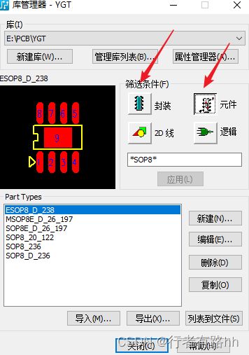
具体情况如下图所示,

解决办法:
(1)复用模块器件的位号与PCB内的位号更改成一样的。
(2)复用模块的器件封装跟PCB中的封装更改成一样的。
博主专注职场硬件设计,如果文章对你有帮助,请关注,点赞,收藏。成长路上有前行者。博主将会定期或不定期分享PADS,Allegro设计技巧和经验。
The PADS Layout user interface is designed for ease of use and efficiency. PADS Layout is designed to meet the needs of the power user, while keeping the beginner in mind. PADS Layout’s interface and interaction are similar to other Windows ™ applications. You can interact with PADS Layout using the keyboard, menus, toolbars, and shortcut menus.
To change the unit of measure to inches, mils (default setting), or metric units, click Options on the Tools menu. The Design Units settings are on the Global >General page of the Options dialog box. Leave the current setting of Mils.
During the many phases of the PCB process, you may want to select only specific objects. For example, during component placement you may want to limit selections to components and during interactive routing you may want to limit selections to connections or routes.
To accommodate this working preference, there is a Selection Filter. With theSelection Filter, you can specify which design objects are selectable. Items turnedoff in the list can't be selected.
You display attributes in the design as text labels. You can also add additionallabels to accommodate different size and location requirements for referencedesignators. The visibility and position of each label is managed within the Layout Editor.
You can predefine locations for attribute labels by adding placeholder labels in the PCB decal. The placeholders act as the defaults for new labels added or made visible in the Layout Editor.
Position the Name and Type labels in the decal where the text will not be obscured when visible.
1. Select button .
2. With nothing selected, right-click and click Select Text/Drafting.
3. Select each label and to move it press Ctrl+E.
4. Place them in the approximate location shown in the "Creating a PCB Decal"
section at the beginning of the tutorial.
5. Click to complete the moves.