- 【嵌入式电机控制#15】电流闭环控制(二):电流采样
Cyber耐提克
嵌入式电机控制系统电机控制嵌入式系统控制算法单片机
代码解析(1)main.c中ADC的DMA中断回调voidHAL_ADC_ConvCpltCallback(ADC_HandleTypeDef*hadc){__IOuint16_tConvCnt=0;__IOint32_tADConv=0;//这里其实没必要用IO定义,变量与外设寄存器无直接交互HAL_ADC_Stop_DMA(hadc);//注意:对于信号传递速度极快的DMA,即使你用了HT中断
- 【亲测免费】 CAN总线嵌入式开发——从入门到实践:开启智能通信新篇章
邴洁沫Edna
CAN总线嵌入式开发——从入门到实践:开启智能通信新篇章去发现同类优质开源项目:https://gitcode.com/项目介绍在现代嵌入式系统中,CAN(ControllerAreaNetwork)总线技术因其高效、可靠的通信能力而备受青睐。为了帮助广大开发者、电子工程师以及对CAN总线技术感兴趣的学生和研究人员更好地掌握这一技术,我们推出了“CAN总线嵌入式开发——从入门到实践”项目。本项目不
- 基于单片机智能插座设计/智能开关
传送门其他作品题目速选一览表其他作品题目功能速览概述随着我国的电子计算机技术的快速发展以及居民对现实生活的要求也在不断提升,所以很多智能化的产品开始慢慢出现。本次设计主要是以物联网为基础,设计一个支持远程控制的智能插座。研究此项目是因为物联网预示了对未来互联网的一种发展趋势它可以让我们的生活变得更加便捷,所以想通过本次设计真正意义上去感受智能产品的魅力;更加深刻了解单片机以及嵌入式操作系的主要特点
- Electron实现“仅首次运行时创建SQLite数据库”
几道之旅
数据库electronsqlite
在桌面应用中,SQLite因其轻量、嵌入式特性成为本地存储的热门选择。但若重复初始化数据库,会导致数据覆盖或冗余。本文将详解如何让Electron应用仅在首次启动时创建SQLite数据库,后续启动直接连接现有库。一、核心逻辑与实现原理核心思路:通过检测数据库文件是否存在,决定是否执行建表操作。关键技术点:路径管理:使用Electron的app.getPath('userData')获取用户数据目录
- 嵌入式学习-PyTorch(8)-day24
LGGGGGQ
学习pytorch深度学习
torch.optim优化器torch.optim是PyTorch中用于优化神经网络参数的模块,里面实现了一系列常用的优化算法,比如SGD、Adam、RMSprop等,主要负责根据梯度更新模型的参数。️核心组成1.常用优化器优化器作用典型参数torch.optim.SGD标准随机梯度下降,支持momentumlr,momentum,weight_decaytorch.optim.Adam自适应学习
- 嵌入式学习-PyTorch(3)-day20
LGGGGGQ
学习pytorch人工智能
transforms结构及用法transforms.yp是一个工具箱就是将一个特定格式的图片经过这个工具的到想要的变换Tensor数据类型一、transforms的使用(Python)fromPILimportImagefromtorch.utils.tensorboardimportSummaryWriterfromtorchvisionimporttransformswriter=Summar
- 嵌入式学习-PyTorch(4)-day21
LGGGGGQ
学习
1、torchvision中数据集的使用认识官方的一些数据集Datasets—Torchvision0.22documentation试了一下CIFAR10数据集,知道了如何下载官方数据集和展示他们去tensorboard中importtorchvisionfromtorch.utils.tensorboardimportSummaryWriter#处理数据集dataset_transform=t
- 基于单片机宠物喂食器/智能宠物窝/智能饲养
传送门其他作品题目速选一览表其他作品题目功能速览概述深夜加班时,你是否担心家中宠物饿肚子?出差旅途中,是否焦虑宠物无人照看?这些养宠族的共同痛点,正被一枚小小的单片机悄然化解。作为智慧宠物家居的核心设备,智能喂食器已从“定时撒粮”的机械玩具,进化成融合嵌入式控制、物联网通信、健康管理的科技终端。本文将深入拆解基于单片机的喂食器设计:从STM32主控芯片的选型,到0.5g精度的闭环投喂算法;从ESP
- 关于字符编辑器vi、vim版本的安装过程及其常用命令:
DIY机器人工房
编辑器vimlinux嵌入式硬件DIY机器人工房stm32单片机
1.编辑器1.1图形编辑器平时常见的编辑器都是图形编辑器,比如记事本、notepad、office、wps等,图形编辑器的意思就是这些编辑器带有图形界面,有菜单选项。比如最简单的Windows的记事本:记事本当然,编程时不可能使用记事本来写代码,常用的专业编程IDE有vsCode、qtCreator等,常用的专业编辑器有sumlime、notepad++、vim等,它们各有所长。其中,在嵌入式开发
- 边缘智能革命:嵌入式机器学习如何让万物“思考”
万能小贤哥
机器学习人工智能
当智能手表精准识别你的健身动作,工业传感器预测设备故障于毫秒之间,农业传感器自动调节灌溉水量——这些并非科幻场景,而是嵌入式机器学习(EmbeddedMachineLearning,或TinyML)正在悄然重塑的现实。这场发生在设备边缘的智能革命,正将AI从云端的数据中心拉近到我们指尖的每一台设备中。一、嵌入式机器学习:定义与核心价值嵌入式机器学习是指在资源极端受限的微控制器(MCU)、微处理器(
- 暑期自学嵌入式——Day02(C语言阶段)
一位搞嵌入式的 genius
嵌入式自学专栏linux嵌入式C语言
点关注不迷路哟。你的点赞、收藏,一键三连,是我持续更新的动力哟!!!主页:一位搞嵌入式的genius-CSDN博客https://blog.csdn.net/m0_73589512?spm=1000.2115.3001.5343目录Day02→数据类型(上)数据类型分类基本数据类型整形数据类型字符型数据类型实型数据类型构造数据类型特殊数据类型布尔类型详解基本概念使用注意事项预处理分析知识小结Day
- 暑期自学嵌入式——Day03(C语言阶段)
一位搞嵌入式的 genius
嵌入式自学专栏c语言开发语言linux嵌入式C语言
个人主页:一位搞嵌入式的genius-CSDN博客https://blog.csdn.net/m0_73589512?spm=1010.2135.3001.5343点关注不迷路哟。你的点赞、收藏,一键三连,是我持续更新的动力哟!!!目录Day03:输入输出(上)Day03→嵌入式开发输入输出(上)知识纲要数据输出1)C语言IO特性2)字符输出函数(putchar)例题:putchar函数应用3)编
- 暑期自学嵌入式——Day04(C语言阶段)
一位搞嵌入式的 genius
嵌入式自学专栏嵌入式C语言linux
点关注不迷路哟。你的点赞、收藏,一键三连,是我持续更新的动力哟!!!目录C语言控制语句控制语句if(上)一、控制语句分类1.基本结构与学习要求2.分支语句3.循环语句4.学习方法建议二、分支语句:if-else详解1.if语句概述2.if语句的常见形式(1)简化形式(省略else)(2)阶梯形式(elseif多分支)3.应用案例:输入分数评级题目要求设计思路与代码实现关键解析4.if语句的嵌套形式
- 数据库、HTML
一、数据库数据库文件与普通文件区别:普通文件对数据管理(增删改查)效率低2.数据库对数据管理效率高,使用方便常用数据库:1.关系型数据库:将复杂的数据结构简化为二维表格形式大型:0racle、DB2中型:MySq1、sQLServer小型:Sqlite2.非关系型数据库以键值对存储,且结构不固定。//JSONRedisMongoDB嵌入式数据库:sqlite3:stu.db1.开源免费,c语言开发
- 【RK3568 嵌入式linux QT开发笔记】 二维码开源库 libqrencode 交叉静态编译和使用
本文参考文章:https://blog.csdn.net/qq_41630102/article/details/108306720参考文章有些地方描述的有疏漏,导致笔者学习过程中,编译的.a文件无法在RK3568平台运行,故写本文做了修正,以下仅是自我学习的笔记,没有写的很详细。一:下载软件包https://download.csdn.net/download/qq_41630102/12781
- QT 交叉编译环境下,嵌入式设备显示字体大小和QT Creator 桌面显示不一致问题解决
第一步:发送fc-list命令,查找嵌入式环境下支持的字库第二步为每个控件指定字库文件,以label控件为例:intfontId=QFontDatabase::addApplicationFont("/usr/share/fonts/source-han-sans-cn/SourceHanSansCN-Normal.otf");if(fontId==-1){//qDebug()label->set
- 内存受限编程:从原理到实践的全面指南
景彡先生
C++进阶c++缓存
在嵌入式系统、物联网设备、移动应用等场景中,内存资源往往极为有限。如何在内存受限的环境中设计高效、稳定的程序,是每个开发者都可能面临的挑战。本文将从硬件原理、操作系统机制、算法优化到代码实现技巧,全面解析内存受限编程的核心技术。一、内存受限环境概述1.1典型内存受限场景场景可用内存范围典型应用8位单片机几KB-64KB传感器节点、简单控制器32位嵌入式系统64KB-512MB智能家居设备、工业控制
- 嵌入式单片机开发实战指南: 从RISC-V到TinyML全栈技术
CodeMicro
单片机单片机risc-v嵌入式硬件
前言:嵌入式单片机的2025年技术浪潮2025年,嵌入式系统正经历开源架构与边缘智能的双重革命。RISC-V指令集打破ARM垄断,国产芯片如兆易创新GD32VF103、先楫HPM6750实现工业级可靠性;TinyML技术让STM32L4系列在1MB内存下运行神经网络;低功耗设计使物联网节点电池寿命突破10年。本文将从架构选型→开发环境→核心技术→实战项目,全方位拆解嵌入式开发的热门技术,带你从入门
- STM32 USB开发详解:CDC虚拟串口与HID键盘鼠标(基于CubeUSB库)
景彡先生
STM32stm32计算机外设嵌入式硬件
前言:STM32的USB功能为何重要?在嵌入式开发中,设备与外界通信的方式多种多样(UART、SPI、I2C等),但USB凭借"即插即用"、"高速传输"和"供电能力"三大优势,成为设备与PC/手机通信的首选方案。STM32大部分中高端型号(如F103C8T6、F407IGH6、L431RCT6等)都集成了USB外设,支持从机、主机或OTG模式,可实现虚拟串口、键盘、鼠标等多种功能。本文聚焦STM3
- 【C++基础】内存对齐原则与性能影响:面试高频考点与真题解析
byte轻骑兵
#C++深度探索与实战专栏面试职场和发展
在计算机系统中,内存对齐是影响程序性能和跨平台兼容性的重要因素。无论是校招还是社招,内存对齐相关问题几乎是C/C++、嵌入式开发、操作系统等岗位的必考题。掌握内存对齐的原理和应用,不仅能应对面试,更是理解现代计算机体系结构的关键。一、内存对齐的基本概念1.1什么是内存对齐?内存对齐是指数据在内存中存储时,其起始地址必须是某个特定值(通常是数据类型大小的倍数)。例如,4字节的int类型变量应存储在4
- OpenHarmony解读之设备认证:解密流程全揭秘
陈乔布斯
HarmonyOS鸿蒙开发OpenHarmonyharmonyosopenHarmony嵌入式硬件鸿蒙开发respons
往期推文全新看点(文中附带最新·鸿蒙全栈学习笔记)①鸿蒙应用开发与鸿蒙系统开发哪个更有前景?②嵌入式开发适不适合做鸿蒙南向开发?看完这篇你就了解了~③对于大前端开发来说,转鸿蒙开发究竟是福还是祸?④鸿蒙岗位需求突增!移动端、PC端、IoT到底该怎么选?⑤记录一场鸿蒙开发岗位面试经历~⑥持续更新中……一、概述本文重点介绍客户端收到end响应消息之后的处理过程。二、源码分析这一模块的源码位于:/bas
- AUTOSAR汽车电子嵌入式编程精讲300篇-基于 FPGA 的 CAN 控制器设计与验证(续)
格图素书
汽车fpga开发
目录3CAN控制器的设计3.1CAN的模块构成3.2CPI模块3.2.1CPI模块总设计3.2.2位时序设计3.2.3发送模块设计3.2.4接收模块设计3.2.5错误处理模块设计3.2.6过载帧模块设计3.3CAN控制器的操作模式4CAN控制器的验证4.1基于Vivado软件的CAN控制器仿真4.1.1CAN控制器配置及地址打包4.1.2其余端口配置说明4.1.3Testbench编写说明4.1.
- 【第三十二天】STM32 平台全景解析与型号选择实战指南
观熵
每日一练:嵌入式C++开发365天stm32嵌入式硬件单片机学习C++
STM32平台全景解析与型号选择实战指南关键词:STM32、MCU选型、STM32F1、STM32G4、STM32H7、Flash/RAM、外设资源、封装选型、低功耗方案、嵌入式平台摘要:STM32系列是目前嵌入式开发中应用最广泛的ARMCortex-M微控制器平台之一,覆盖从入门级控制器到高性能边缘处理器的多种应用场景。本文从STM32的平台分类、架构演进、性能指标、外设组合、功耗管理等角度展开
- 摄像驱动会接触到的单词(想起来就更新)3
空与实的极致
嵌入式硬件经验分享计算机视觉视觉检测
工作单词delivers交付;传递assignment分配;任务;指派firmware固件stack栈integrate整合superspeed超高速embedded嵌入式development研发、开发;发展kit装备;配套元件;成套工具platforms平台、站台device设备、物品、器械peripheral外围设备;外围的;次要的access通道;入口;机会interface接口;界面se
- 嵌入式系统LCD显示模块编程实践
本文还有配套的精品资源,点击获取简介:本文档提供了一个具有800x480分辨率的3.5英寸液晶显示模块LW350AC9001的驱动程序代码,以及嵌入式系统中使用C/C++语言进行硬件编程的实践指南。该模块的2mm厚度使其适用于空间受限的便携式设备。内容包括驱动程序源代码、硬件控制接口使用方法,以及如何在嵌入式系统中进行图形处理、电源管理与性能优化。1.嵌入式系统原理1.1嵌入式系统概念嵌入式系统是
- ARM嵌入式可编程控制器技术开发
拉勾科研工作室
arm开发
PLC自动化设计|毕业设计指导|工业自动化解决方案✨专业领域:PLC程序设计与调试工业自动化控制系统HMI人机界面开发工业传感器应用电气控制系统设计工业网络通信擅长工具:西门子S7系列PLC编程三菱/欧姆龙PLC应用触摸屏界面设计电气CAD制图工业现场总线技术自动化设备调试主要内容:PLC控制系统设计工业自动化方案规划电气原理图绘制控制程序编写与调试毕业论文指导毕业设计题目与程序设计✅具体问题可以
- 上位机知识篇---文件系统
Atticus-Orion
上位机知识篇文件系统windowslinuxFATNTFSext4ZFS
文章目录前言1.FAT(FileAllocationTable)版本FAT12FAT16FAT32优势兼容性好简单轻量适合小文件存储劣势不支持大文件性能较差缺乏高级功能使用场景2.NTFS(NewTechnologyFileSystem)优势支持大文件和大分区高性能日记功能权限控制劣势兼容性差不适合嵌入式设备使用场景3.exFAT(ExtendedFileAllocationTable)优势支持大
- STM32F1系列综合测试程序实践指南
Love Snape
本文还有配套的精品资源,点击获取简介:STM32F1系列微控制器是基于ARMCortex-M3内核的低成本、高性能嵌入式系统解决方案。本综合测试程序旨在帮助初学者快速掌握STM32的基础操作和关键知识点,包括裸机编程、GPIO操作、定时器应用、串行通信、ADC转换、中断处理和Bootloader等。同时,程序将指导学习者熟悉开发环境和理解代码结构,为未来在嵌入式系统开发领域打下坚实的基础。1.ST
- 开源 Arkts 鸿蒙应用 开发(六)数据持久--文件和首选项存储
文章的目的为了记录使用Arkts进行Harmonyapp开发学习的经历。本职为嵌入式软件开发,公司安排开发app,临时学习,完成app的开发。开发流程和要点有些记忆模糊,赶紧记录,防止忘记。相关链接:开源Arkts鸿蒙应用开发(一)工程文件分析-CSDN博客开源Arkts鸿蒙应用开发(二)封装库.har制作和应用-CSDN博客开源Arkts鸿蒙应用开发(三)Arkts的介绍-CSDN博客开源Ark
- 嵌入式硬件中电容的基本原理与实现详解02
嵌入式开发星球
单片机项目实战操作之优秀单片机嵌入式硬件
我们今天重点讨论点知识点如下:1.各种种类的电容优缺点对比讲解2.电容的标称值介绍3.电容的单位介绍4.常见的电压信号有哪些?5.电容的耐压值讲解6.电容的容值有哪些?7.12pF、15pF电容常用在什么场合?8.振荡电路中使用的电容常常需要使用什么材质的电容?9.100nF电容常用在什么场合?有什么作用?10.独石电容介绍
- 解线性方程组
qiuwanchi
package gaodai.matrix;
import java.util.ArrayList;
import java.util.List;
import java.util.Scanner;
public class Test {
public static void main(String[] args) {
Scanner scanner = new Sc
- 在mysql内部存储代码
annan211
性能mysql存储过程触发器
在mysql内部存储代码
在mysql内部存储代码,既有优点也有缺点,而且有人倡导有人反对。
先看优点:
1 她在服务器内部执行,离数据最近,另外在服务器上执行还可以节省带宽和网络延迟。
2 这是一种代码重用。可以方便的统一业务规则,保证某些行为的一致性,所以也可以提供一定的安全性。
3 可以简化代码的维护和版本更新。
4 可以帮助提升安全,比如提供更细
- Android使用Asynchronous Http Client完成登录保存cookie的问题
hotsunshine
android
Asynchronous Http Client是android中非常好的异步请求工具
除了异步之外还有很多封装比如json的处理,cookie的处理
引用
Persistent Cookie Storage with PersistentCookieStore
This library also includes a PersistentCookieStore whi
- java面试题
Array_06
java面试
java面试题
第一,谈谈final, finally, finalize的区别。
final-修饰符(关键字)如果一个类被声明为final,意味着它不能再派生出新的子类,不能作为父类被继承。因此一个类不能既被声明为 abstract的,又被声明为final的。将变量或方法声明为final,可以保证它们在使用中不被改变。被声明为final的变量必须在声明时给定初值,而在以后的引用中只能
- 网站加速
oloz
网站加速
前序:本人菜鸟,此文研究总结来源于互联网上的资料,大牛请勿喷!本人虚心学习,多指教.
1、减小网页体积的大小,尽量采用div+css模式,尽量避免复杂的页面结构,能简约就简约。
2、采用Gzip对网页进行压缩;
GZIP最早由Jean-loup Gailly和Mark Adler创建,用于UNⅨ系统的文件压缩。我们在Linux中经常会用到后缀为.gz
- 正确书写单例模式
随意而生
java 设计模式 单例
单例模式算是设计模式中最容易理解,也是最容易手写代码的模式了吧。但是其中的坑却不少,所以也常作为面试题来考。本文主要对几种单例写法的整理,并分析其优缺点。很多都是一些老生常谈的问题,但如果你不知道如何创建一个线程安全的单例,不知道什么是双检锁,那这篇文章可能会帮助到你。
懒汉式,线程不安全
当被问到要实现一个单例模式时,很多人的第一反应是写出如下的代码,包括教科书上也是这样
- 单例模式
香水浓
java
懒汉 调用getInstance方法时实例化
public class Singleton {
private static Singleton instance;
private Singleton() {}
public static synchronized Singleton getInstance() {
if(null == ins
- 安装Apache问题:系统找不到指定的文件 No installed service named "Apache2"
AdyZhang
apachehttp server
安装Apache问题:系统找不到指定的文件 No installed service named "Apache2"
每次到这一步都很小心防它的端口冲突问题,结果,特意留出来的80端口就是不能用,烦。
解决方法确保几处:
1、停止IIS启动
2、把端口80改成其它 (譬如90,800,,,什么数字都好)
3、防火墙(关掉试试)
在运行处输入 cmd 回车,转到apa
- 如何在android 文件选择器中选择多个图片或者视频?
aijuans
android
我的android app有这样的需求,在进行照片和视频上传的时候,需要一次性的从照片/视频库选择多条进行上传
但是android原生态的sdk中,只能一个一个的进行选择和上传。
我想知道是否有其他的android上传库可以解决这个问题,提供一个多选的功能,可以使checkbox之类的,一次选择多个 处理方法
官方的图片选择器(但是不支持所有版本的androi,只支持API Level
- mysql中查询生日提醒的日期相关的sql
baalwolf
mysql
SELECT sysid,user_name,birthday,listid,userhead_50,CONCAT(YEAR(CURDATE()),DATE_FORMAT(birthday,'-%m-%d')),CURDATE(), dayofyear( CONCAT(YEAR(CURDATE()),DATE_FORMAT(birthday,'-%m-%d')))-dayofyear(
- MongoDB索引文件破坏后导致查询错误的问题
BigBird2012
mongodb
问题描述:
MongoDB在非正常情况下关闭时,可能会导致索引文件破坏,造成数据在更新时没有反映到索引上。
解决方案:
使用脚本,重建MongoDB所有表的索引。
var names = db.getCollectionNames();
for( var i in names ){
var name = names[i];
print(name);
- Javascript Promise
bijian1013
JavaScriptPromise
Parse JavaScript SDK现在提供了支持大多数异步方法的兼容jquery的Promises模式,那么这意味着什么呢,读完下文你就了解了。
一.认识Promises
“Promises”代表着在javascript程序里下一个伟大的范式,但是理解他们为什么如此伟大不是件简
- [Zookeeper学习笔记九]Zookeeper源代码分析之Zookeeper构造过程
bit1129
zookeeper
Zookeeper重载了几个构造函数,其中构造者可以提供参数最多,可定制性最多的构造函数是
public ZooKeeper(String connectString, int sessionTimeout, Watcher watcher, long sessionId, byte[] sessionPasswd, boolea
- 【Java命令三】jstack
bit1129
jstack
jstack是用于获得当前运行的Java程序所有的线程的运行情况(thread dump),不同于jmap用于获得memory dump
[hadoop@hadoop sbin]$ jstack
Usage:
jstack [-l] <pid>
(to connect to running process)
jstack -F
- jboss 5.1启停脚本 动静分离部署
ronin47
以前启动jboss,往各种xml配置文件,现只要运行一句脚本即可。start nohup sh /**/run.sh -c servicename -b ip -g clustername -u broatcast jboss.messaging.ServerPeerID=int -Djboss.service.binding.set=p
- UI之如何打磨设计能力?
brotherlamp
UIui教程ui自学ui资料ui视频
在越来越拥挤的初创企业世界里,视觉设计的重要性往往可以与杀手级用户体验比肩。在许多情况下,尤其对于 Web 初创企业而言,这两者都是不可或缺的。前不久我们在《右脑革命:别学编程了,学艺术吧》中也曾发出过重视设计的呼吁。如何才能提高初创企业的设计能力呢?以下是 9 位创始人的体会。
1.找到自己的方式
如果你是设计师,要想提高技能可以去设计博客和展示好设计的网站如D-lists或
- 三色旗算法
bylijinnan
java算法
import java.util.Arrays;
/**
问题:
假设有一条绳子,上面有红、白、蓝三种颜色的旗子,起初绳子上的旗子颜色并没有顺序,
您希望将之分类,并排列为蓝、白、红的顺序,要如何移动次数才会最少,注意您只能在绳
子上进行这个动作,而且一次只能调换两个旗子。
网上的解法大多类似:
在一条绳子上移动,在程式中也就意味只能使用一个阵列,而不使用其它的阵列来
- 警告:No configuration found for the specified action: \'s
chiangfai
configuration
1.index.jsp页面form标签未指定namespace属性。
<!--index.jsp代码-->
<%@taglib prefix="s" uri="/struts-tags"%>
...
<s:form action="submit" method="post"&g
- redis -- hash_max_zipmap_entries设置过大有问题
chenchao051
redishash
使用redis时为了使用hash追求更高的内存使用率,我们一般都用hash结构,并且有时候会把hash_max_zipmap_entries这个值设置的很大,很多资料也推荐设置到1000,默认设置为了512,但是这里有个坑
#define ZIPMAP_BIGLEN 254
#define ZIPMAP_END 255
/* Return th
- select into outfile access deny问题
daizj
mysqltxt导出数据到文件
本文转自:http://hatemysql.com/2010/06/29/select-into-outfile-access-deny%E9%97%AE%E9%A2%98/
为应用建立了rnd的帐号,专门为他们查询线上数据库用的,当然,只有他们上了生产网络以后才能连上数据库,安全方面我们还是很注意的,呵呵。
授权的语句如下:
grant select on armory.* to rn
- phpexcel导出excel表简单入门示例
dcj3sjt126com
PHPExcelphpexcel
<?php
error_reporting(E_ALL);
ini_set('display_errors', TRUE);
ini_set('display_startup_errors', TRUE);
if (PHP_SAPI == 'cli')
die('This example should only be run from a Web Brows
- 美国电影超短200句
dcj3sjt126com
电影
1. I see. 我明白了。2. I quit! 我不干了!3. Let go! 放手!4. Me too. 我也是。5. My god! 天哪!6. No way! 不行!7. Come on. 来吧(赶快)8. Hold on. 等一等。9. I agree。 我同意。10. Not bad. 还不错。11. Not yet. 还没。12. See you. 再见。13. Shut up!
- Java访问远程服务
dyy_gusi
httpclientwebservicegetpost
随着webService的崛起,我们开始中会越来越多的使用到访问远程webService服务。当然对于不同的webService框架一般都有自己的client包供使用,但是如果使用webService框架自己的client包,那么必然需要在自己的代码中引入它的包,如果同时调运了多个不同框架的webService,那么就需要同时引入多个不同的clien
- Maven的settings.xml配置
geeksun
settings.xml
settings.xml是Maven的配置文件,下面解释一下其中的配置含义:
settings.xml存在于两个地方:
1.安装的地方:$M2_HOME/conf/settings.xml
2.用户的目录:${user.home}/.m2/settings.xml
前者又被叫做全局配置,后者被称为用户配置。如果两者都存在,它们的内容将被合并,并且用户范围的settings.xml优先。
- ubuntu的init与系统服务设置
hongtoushizi
ubuntu
转载自:
http://iysm.net/?p=178 init
Init是位于/sbin/init的一个程序,它是在linux下,在系统启动过程中,初始化所有的设备驱动程序和数据结构等之后,由内核启动的一个用户级程序,并由此init程序进而完成系统的启动过程。
ubuntu与传统的linux略有不同,使用upstart完成系统的启动,但表面上仍维持init程序的形式。
运行
- 跟我学Nginx+Lua开发目录贴
jinnianshilongnian
nginxlua
使用Nginx+Lua开发近一年的时间,学习和实践了一些Nginx+Lua开发的架构,为了让更多人使用Nginx+Lua架构开发,利用春节期间总结了一份基本的学习教程,希望对大家有用。也欢迎谈探讨学习一些经验。
目录
第一章 安装Nginx+Lua开发环境
第二章 Nginx+Lua开发入门
第三章 Redis/SSDB+Twemproxy安装与使用
第四章 L
- php位运算符注意事项
home198979
位运算PHP&
$a = $b = $c = 0;
$a & $b = 1;
$b | $c = 1
问a,b,c最终为多少?
当看到这题时,我犯了一个低级错误,误 以为位运算符会改变变量的值。所以得出结果是1 1 0
但是位运算符是不会改变变量的值的,例如:
$a=1;$b=2;
$a&$b;
这样a,b的值不会有任何改变
- Linux shell数组建立和使用技巧
pda158
linux
1.数组定义 [chengmo@centos5 ~]$ a=(1 2 3 4 5) [chengmo@centos5 ~]$ echo $a 1 一对括号表示是数组,数组元素用“空格”符号分割开。
2.数组读取与赋值 得到长度: [chengmo@centos5 ~]$ echo ${#a[@]} 5 用${#数组名[@或
- hotspot源码(JDK7)
ol_beta
javaHotSpotjvm
源码结构图,方便理解:
├─agent Serviceab
- Oracle基本事务和ForAll执行批量DML练习
vipbooks
oraclesql
基本事务的使用:
从账户一的余额中转100到账户二的余额中去,如果账户二不存在或账户一中的余额不足100则整笔交易回滚
select * from account;
-- 创建一张账户表
create table account(
-- 账户ID
id number(3) not null,
-- 账户名称
nam

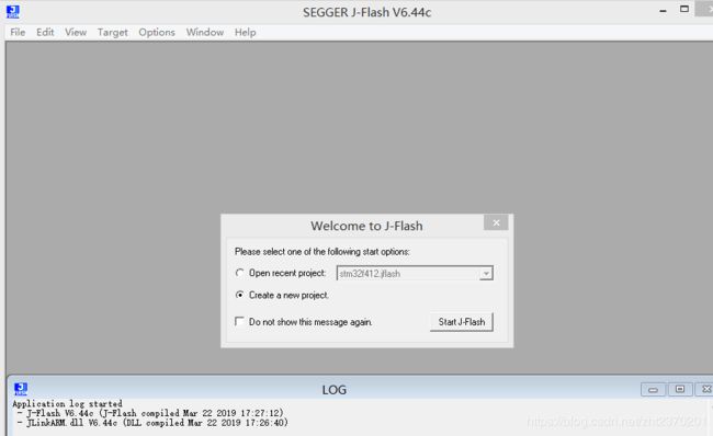
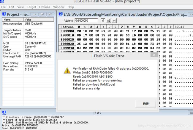
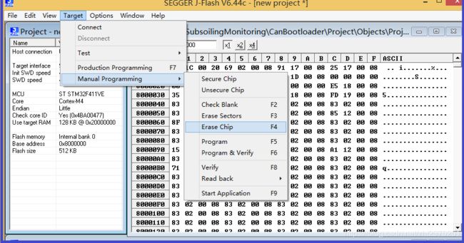
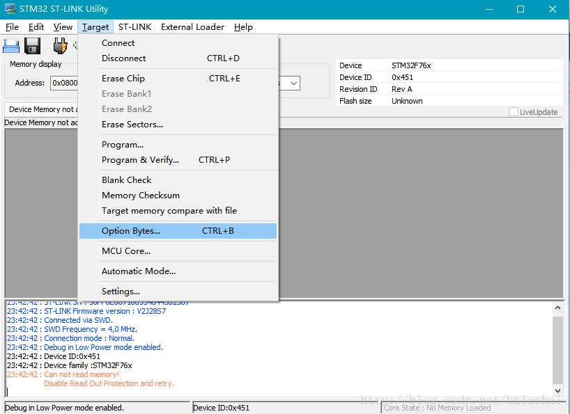
 通过SWD将芯片与JLink连接后,选择Target-Connect即可连接成功。