- Verilog系统函数实现单精度float、双精度doble浮点类型和整型之间互相转换
whik1194
XilinxFPGAZYNQverilogsystemverilog
标准verilog支持双精度double类型和十六进制64位数据相互转换,使用$realtobits和$bitstoreal系统函数使用示例://test_tb.v`timescale1ns/1psmoduletest_tb;realdata_real;reg[63:0]data_hex;initialbegindata_real=0;data_hex=0;data_real=1234.56789
- I2C协议与FPGA开发教程_VHDL/Verilog实现
侯昂
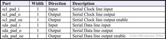
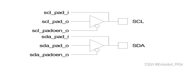
本文还有配套的精品资源,点击获取简介:本压缩包文件包含了I2C协议的学习资料,特别是针对FPGA开发的实验教程。内容涵盖了I2C基础知识、通信模式、总线仲裁机制,以及用VHDL和Verilog语言实现I2C控制器的方法。教程还包括在FPGA平台配置I2C接口的详细步骤和实验指导,帮助读者深入理解I2C协议,并在FPGA上实现其控制。1.I2C协议基础介绍I2C(Inter-IntegratedCi
- verilog Matlab GPS C/A码发生器.
today_typ
verilog学习日志开发语言matlab经验分享fpga开发
本文所涉文献资料均为开源免费,参考文献、声明链接等均写在文末。1.C/A码简要介绍GPS卫星信号包括载波信号、测距码和数据码.其中的测码粗码即C/A码(CoarseAcquisitionCode)除了作为粗测码外,还由于其具有码长短,易于捕获的特点而作为GPS卫星信号的捕获码,因此C/A码是GPS信号捕获以及接收机实现的基础。[1]GPS系统中使用了两种伪随机码,一种是时钟速率为10.23MHz用
- Linux虚拟机磁盘扩容
会飞的土拨鼠呀
Linux运维技巧运维学习笔记linuxcentos运维
1.查看磁盘信息lsblk2.查看待分区的磁盘的信息fdisk-l3.查看磁盘情况:打印可用空间parted/dev/sdaprintfree4.分配剩余的可用空间将剩余的可用空间分配到/dev/sda2,根据实际修改磁盘resizepart中的2只的是第二个分区即:/dev/sda2100%将所有的空闲空间分配给/dev/sda2,也可以用单位和百分比parted/dev/sdaresizepa
- Quartus Prime 仿真相关报错解决方法
门外的兔子
问题解决fpga开发嵌入式硬件
出现如图相关报错是因为文件路径的问题解决方法如下:第一步打开仿真设置第二步检查如图所示路径是否正确即对应.VMF文件保存的路径复制粘贴可见上方文本如下quartus_eda--gen_testbench--tool=modelsim_oem--format=verilog--write_settings_files=offProject-cProject--vector_source="D:/Kt
- Linux 如何使用fdisk进行磁盘相关的操作
孤客网络科技工作室
linux运维服务器
简介fdisk命令是Linux中用于管理磁盘分区的强大文本实用程序。它可以创建、删除、调整大小和修改硬盘上的分区。基本语法fdisk[options]:要管理的磁盘,例如/dev/sda、/dev/nvme0n1或/dev/vda示例用法列出所有分区将显示所有可用的磁盘及其分区,包括它们的大小和文件系统fdisk-l示例输出Disk/dev/sda:500GBSectorsize(logical/
- 【软件工具】如何在在 CentOS 中安装 Python 3
阿寻寻
软件工具pythoncentos开发语言
如何在在CentOS中安装Python3一、方法1:使用`yum`安装(CentOS7及以上)步骤:方法2:使用SoftwareCollections(SCL)安装(适用于CentOS7)步骤:方法3:从源代码编译安装(适用于高级用户)步骤:方法4:使用`pyenv`安装(适用于多版本管理)安装`pyenv`:总结二、1.**开发工具包**2.**必备依赖包**3.**Python特定依赖包**4
- 数码管扫描显示verilog_如何开始Xilinx FPGA开发之旅 第二课 EGO1数码管与键盘
weixin_39869959
数码管扫描显示verilog
庚子年,我们的EGO1在疫情当中作为口袋实验平台成为了众多高校的复课利器。其中的成功案例更是得到了新华社网媒与CCTV教育频道的报道。借此东风,为了让更多的老师与学生熟悉了解Xilinx,更好的入门学习FPGA知识,我们的师资培训直播已开设EGO1专题直播,欢迎新老朋友跟踪关注。第二课----EGO1数码管与键盘本周的直播我们将介绍EGO1的外设使用案例,介绍数码管扫描的原理和PS/2协议。并教大
- FPGA入门学习之Vivado-数码管驱动设计实验
ZdqDeveloper
fpga开发学习FPGA
在本篇文章中,我们将介绍如何使用Vivado软件进行FPGA的数码管驱动设计实验。数码管是一种常见的输出设备,用于显示数字或字符等信息。通过本实验,您将学习如何使用FPGA来控制数码管的显示,并编写相应的Verilog代码。实验准备:Vivado软件的安装和配置。FPGA开发板(如Xilinx的Basys3)。实验步骤:步骤1:创建新工程打开Vivado软件,并选择"CreateProject"来
- 基于 FPGA 的简易 OFDM 系统 Verilog 实现
鱼弦
人工智能时代fpga开发
基于FPGA的简易OFDM系统Verilog实现介绍OFDM(正交频分复用)是一种广泛应用于无线通信系统的多载波调制技术,用于提升数据传输效率和抗干扰能力。通过利用多个正交子载波,OFDM将高速数据流分散到多个低速数据流上进行并行传输。FPGA提供了并行处理能力,是实现实时OFDM系统的理想平台。应用使用场景无线通信:如Wi-Fi、LTE和5G中的数据传输。数字广播:用于DAB和DVB等广播系统。
- STM32完全学习——0V5640的JPEG模式采集
小A159
学习
一、写在前面我参考的是买开发板的时候,普中送的资料里面的源码,他那个是用标准库写的,我将他的代码移植到了HAL库,有一些不一样的地方。由于标准库和HAL库的差别造成的。二、编程思路首先初始化OV5640模块,使用的是SCCB总线,和I2C很像,具体的就不说了,再就是将OV5640设置成JPEG输出模式,然后就是调整OV5640输出的图像的大小。下来就是开启DMA传输。然后每捕获一帧图像,DCMI会
- <sa8650>sa8650 qcxserver-之-摄像头传感器VB56G4A驱动开发<1>
waterAdmin
驱动开发linuxxml车载系统视觉检测汽车
<sa8650>sa8650qcxserver-之-摄像头传感器VB56G4A驱动开发一、前言二、QCX架构三、QCX传感器驱动程序定制开发3.1sensor硬件接口3.2sensor配置文件3.2.1cameraconfig.c3.2.2cameraconfigsa8650_water.c3.2.3新增编译MK3.2.4参数解析3.2.4.1structCameraConfigI2CDevice
- Microchip 系列:SAM L 系列 (基于 ARM Cortex-M0+)_(7).外设驱动开发
kkchenkx
单片机开发arm开发驱动开发架构java数据库嵌入式硬件
外设驱动开发在外设驱动开发中,我们将详细介绍如何使用Microchip的SAML系列单片机(基于ARMCortex-M0+)来开发各种外设驱动程序。这部分内容将涵盖常见的外设,如GPIO、UART、SPI、I2C、ADC和DAC等,并提供具体的代码示例和操作步骤。GPIO驱动开发GPIO引脚配置GPIO(GeneralPurposeInput/Output)是单片机中最基本的外设之一。通过配置GP
- 学习yosys(一款开源综合器)
qq85058522
自己动手写CPUfpga开发
安装sudoapt-getinstallyosys#ubuntu22.04仓库里面是yosys-0.9sudoinstallxdot创建脚本show_rtl.ysread_verilogcpu.vhierarchy-topcpuproc;opt;fsm;opt;memory;opt;show-prefixcpu调用脚本yosysshow_rtl.ysverilog代码modulecpu(input
- Verilog边沿检测
csdn_gddf102384398
fpga开发
edge_check.vmoduleedge_check(inputclk,inputin,outputneg_edge,outputpos_edge);regr1=1'd0;regr2=1'd0;assignneg_edge=(~r1)&r2;assignpos_edge=r1&(~r2);always@(posedgeclk)beginr1<=in;r2<=r1;endendmoduletb.
- Verilog呼吸灯项目实战指南
酸甜草莓二侠
本文还有配套的精品资源,点击获取简介:本项目“breathLED.zip”详细介绍了利用Verilog硬件描述语言实现呼吸灯效果的完整流程。从Verilog基础到C语言仿真,再到实际的Verilog仿真、工程建立和硬件烧录,详细讲述了在FPGA设计中的每个关键步骤。涵盖了时钟信号定义、计数器和比较器的设计、Testbench编写、编译综合、布局布线以及最终的硬件烧录与调试。本项目不仅提供了实践指南
- [读书日志]8051软核处理器设计实战(基于FPGA)第六篇:8051软核处理器指令支持添加(verilog)
JoneMaster
JM读书日志系列fpga开发
5.4为主体程序添加指令接下来我们来为主体程序添加指令。在开始之前,我们有必要先把目前的代码展示出来://`defineTYPE8052moduler8051(inputwireclk,inputwirerst,inputwirecpu_en,inputwirecpu_restart,outputregrom_en,outputreg[15:0]rom_addr,inputwire[7:0]rom
- FPGA USB2.0串口通信项目设计与实现
瞬泉
本文还有配套的精品资源,点击获取简介:本项目主要围绕FPGA(Field-ProgrammableGateArray)和Verilog语言,实现USB(通用串行总线)2.0标准的串口通信功能。项目涵盖了从时钟配置到物理层接口的全套设计过程,包括UART通信的帧同步、波特率生成、握手协议等。项目文档和代码可能包含Verilog代码文件、测试平台配置、波形记录文件、编译脚本和用户手册,以助于开发者理解
- Linux 如何使用fdisk进行磁盘相关的操作
linux
简介fdisk命令是Linux中用于管理磁盘分区的强大文本实用程序。它可以创建、删除、调整大小和修改硬盘上的分区。基本语法fdisk[options]:要管理的磁盘,例如/dev/sda、/dev/nvme0n1或/dev/vda示例用法列出所有分区将显示所有可用的磁盘及其分区,包括它们的大小和文件系统fdisk-l示例输出Disk/dev/sda:500GBSectorsize(logical/
- php linux 常用命令,Linux常用命令大全
潘儒锋
phplinux常用命令
Linux常用命令大全,以前收集的系统信息arch显示机器的处理器架构(1)uname-m显示机器的处理器架构(2)uname-r显示正在使用的内核版本dmidecode-q显示硬件系统部件-(SMBIOS/DMI)hdparm-i/dev/hda罗列一个磁盘的架构特性hdparm-tT/dev/sda在磁盘上执行测试性读取操作cat/proc/cpuinfo显示CPUinfo的信息cat/pro
- linux操作命令comm,史上最全的Linux常用命令
云小牙
linux操作命令comm
系统信息arch显示机器的处理器架构(1)uname-m显示机器的处理器架构(2)uname-r显示正在使用的内核版本dmidecode-q显示硬件系统部件-(SMBIOS/DMI)hdparm-i/dev/hda罗列一个磁盘的架构特性hdparm-tT/dev/sda在磁盘上执行测试性读取操作cat/proc/cpuinfo显示CPUinfo的信息cat/proc/interrupts显示中断c
- FPGA开发中的团队协作:构建高效协同的关键路径
whik1194
fpga开发
一、团队成员角色与职责FPGA工程师核心设计:负责FPGA的逻辑设计与代码实现,依据项目需求,运用硬件描述语言(如Verilog或VHDL)完成模块功能编写。例如在设计一个高速数据采集系统时,编写数据采集、缓存及预处理的逻辑代码。功能仿真与验证:使用仿真工具对所编写的代码进行功能验证,确保逻辑设计符合预期。像在完成数字滤波器模块代码后,通过仿真测试不同输入信号下的输出,检查滤波效果。时序分析与优化
- [Linux 基础] -- 内核探究:regmap 机制
BestW2Y
Linux基础linuxregmap
前言:regmap机制是在Linux3.1加入的新特性。主要目的是减少I/O驱动上的重复逻辑代码,提供一种通用的接口来操作底层硬件上的寄存器。比如,之前如果要操作i2c设备的寄存器,我们要调用i2c_transfer接口,要操作spi设备的寄存器,就要调用spi_write/spi_read等接口,如果把它们抽象为regmap结构,那么只要调用regmap_read/regmap_write就可以
- Linux 存储设备和 Ventoy 启动盘制作指南
小白也有IT梦
linux运维服务器
一、Linux存储设备基础知识1.设备路径(/dev)设备路径是Linux系统中物理存储设备的唯一标识,类似设备的"身份证号"。命名规则解析/dev/sda:/dev:device(设备)的缩写,存放设备文件的目录sd:源自SCSIdevice,现在用于表示存储设备a:表示第一个检测到的存储设备数字(如sda1):表示该设备上的分区编号2.挂载点与挂载过程挂载点是访问存储设备内容的入口,本质是一个
- 记录一次 centos 启动失败
__pop_
杂七杂八总览linux运维服务器centos
文章目录现场1分析1现场2分析2搜索实际解决过程现场1一次断电,导致之前能正常启动的centos7.7起不来了有部分log,关键信息如下[1.332724]XFS(sda3):Internalerrorxfs...atlinexxxoffs/xfs/xfs_trans.c[1.332724]XFS(sda3):Corruptionofin-memorydatadetected.Shuttingdo
- 自己动手写CPU - 1
qq85058522
自己动手写CPUfpga开发
电脑,手机,单片机,都有一个核心部件:CPU.今天开始学verilog,就尝试一下动手写一个可以工作的CPU.目标就是可以计算从1加到10等于几?分析一下,大概需要几个指令:LdrAddSubCmpJmp第一步,先写一个运算部件:ALU.modulealu0(input[3:0]op,input[7:0]in1,in2,outputreg[7:0]out1);always@(*)begincase
- 【自用】Verilog笔记
QCCX_bY
笔记
一、语法1、模块moduletest(A,B,C,D,F1,F2);//test为模块名inputA,B,C,D;//输入端口,默认为wire类型信号,一般都是wireoutputF1,F2;//输出端口,默认wirewireF1;//连线reg[2:0]F2;//3bit寄存器endmodulemoduletop_module(inputa,inputb,outputout);//模块实例化语法
- BH1750使用程序
兢兢业业的打野
单片机嵌入式硬件
#include"delay.h"#include"GY30/BH1750FVI.h"typedefunsignedcharBYTE;//BYTEBUF[8];//接收数据缓存区//iic接口初始化/****设置SDA为输出**/voidBH1750_SDA_OUT(void){GPIO_InitTypeDefGPIO_InitStructer;GPIO_InitStructer.GPIO_Pin
- Linux 怎么在储存设备上创建文件系统?
linux
简介Linux中的mkfs命令用于在存储设备(例如分区、逻辑卷或整个磁盘)上创建文件系统。它代表makefilesystem(创建文件系统),是磁盘格式化的基本命令。语法mkfs[options]:目标设备,例如:/dev/sda1,/dev/sdb,/dev/loop0[options]:定制文件系统的选项支持的文件系统ext2/3/4:第二、第三和第四个扩展文件系统(mkfs.ext2、mkf
- 嵌入式驱动开发详解9(platform驱动)
嵌入~狮
Linux驱动驱动开发
文章目录前言platform简介总线驱动设备设备树下的platform驱动在设备树中创建设备节点编写platform驱动后续参考文献前言Linux系统要考虑到驱动的可重用性,提出了驱动的分离与分层这样的软件思路,在这个思路下诞生了我们最常打交道的platform设备驱动,也叫做平台设备驱动。platform简介在实际的驱动开发中,一般I2C主机控制器驱动已经由半导体厂家编写好了,而设备驱动一般也由
- TOMCAT在POST方法提交参数丢失问题
357029540
javatomcatjsp
摘自http://my.oschina.net/luckyi/blog/213209
昨天在解决一个BUG时发现一个奇怪的问题,一个AJAX提交数据在之前都是木有问题的,突然提交出错影响其他处理流程。
检查时发现页面处理数据较多,起初以为是提交顺序不正确修改后发现不是由此问题引起。于是删除掉一部分数据进行提交,较少数据能够提交成功。
恢复较多数据后跟踪提交FORM DATA ,发现数
- 在MyEclipse中增加JSP模板 删除-2008-08-18
ljy325
jspxmlMyEclipse
在D:\Program Files\MyEclipse 6.0\myeclipse\eclipse\plugins\com.genuitec.eclipse.wizards_6.0.1.zmyeclipse601200710\templates\jsp 目录下找到Jsp.vtl,复制一份,重命名为jsp2.vtl,然后把里面的内容修改为自己想要的格式,保存。
然后在 D:\Progr
- JavaScript常用验证脚本总结
eksliang
JavaScriptjavaScript表单验证
转载请出自出处:http://eksliang.iteye.com/blog/2098985
下面这些验证脚本,是我在这几年开发中的总结,今天把他放出来,也算是一种分享吧,现在在我的项目中也在用!包括日期验证、比较,非空验证、身份证验证、数值验证、Email验证、电话验证等等...!
&nb
- 微软BI(4)
18289753290
微软BI SSIS
1)
Q:查看ssis里面某个控件输出的结果:
A MessageBox.Show(Dts.Variables["v_lastTimestamp"].Value.ToString());
这是我们在包里面定义的变量
2):在关联目的端表的时候如果是一对多的关系,一定要选择唯一的那个键作为关联字段。
3)
Q:ssis里面如果将多个数据源的数据插入目的端一
- 定时对大数据量的表进行分表对数据备份
酷的飞上天空
大数据量
工作中遇到数据库中一个表的数据量比较大,属于日志表。正常情况下是不会有查询操作的,但如果不进行分表数据太多,执行一条简单sql语句要等好几分钟。。
分表工具:linux的shell + mysql自身提供的管理命令
原理:使用一个和原表数据结构一样的表,替换原表。
linux shell内容如下:
=======================开始
- 本质的描述与因材施教
永夜-极光
感想随笔
不管碰到什么事,我都下意识的想去探索本质,找寻一个最形象的描述方式。
我坚信,世界上对一件事物的描述和解释,肯定有一种最形象,最贴近本质,最容易让人理解
&
- 很迷茫。。。
随便小屋
随笔
小弟我今年研一,也是从事的咱们现在最流行的专业(计算机)。本科三流学校,为了能有个更好的跳板,进入了考研大军,非常有幸能进入研究生的行业(具体学校就不说了,怕把学校的名誉给损了)。
先说一下自身的条件,本科专业软件工程。主要学习就是软件开发,几乎和计算机没有什么区别。因为学校本身三流,也就是让老师带着学生学点东西,然后让学生毕业就行了。对专业性的东西了解的非常浅。就那学的语言来说
- 23种设计模式的意图和适用范围
aijuans
设计模式
Factory Method 意图 定义一个用于创建对象的接口,让子类决定实例化哪一个类。Factory Method 使一个类的实例化延迟到其子类。 适用性 当一个类不知道它所必须创建的对象的类的时候。 当一个类希望由它的子类来指定它所创建的对象的时候。 当类将创建对象的职责委托给多个帮助子类中的某一个,并且你希望将哪一个帮助子类是代理者这一信息局部化的时候。
Abstr
- Java中的synchronized和volatile
aoyouzi
javavolatilesynchronized
说到Java的线程同步问题肯定要说到两个关键字synchronized和volatile。说到这两个关键字,又要说道JVM的内存模型。JVM里内存分为main memory和working memory。 Main memory是所有线程共享的,working memory则是线程的工作内存,它保存有部分main memory变量的拷贝,对这些变量的更新直接发生在working memo
- js数组的操作和this关键字
百合不是茶
js数组操作this关键字
js数组的操作;
一:数组的创建:
1、数组的创建
var array = new Array(); //创建一个数组
var array = new Array([size]); //创建一个数组并指定长度,注意不是上限,是长度
var arrayObj = new Array([element0[, element1[, ...[, elementN]]]
- 别人的阿里面试感悟
bijian1013
面试分享工作感悟阿里面试
原文如下:http://greemranqq.iteye.com/blog/2007170
一直做企业系统,虽然也自己一直学习技术,但是感觉还是有所欠缺,准备花几个月的时间,把互联网的东西,以及一些基础更加的深入透析,结果这次比较意外,有点突然,下面分享一下感受吧!
&nb
- 淘宝的测试框架Itest
Bill_chen
springmaven框架单元测试JUnit
Itest测试框架是TaoBao测试部门开发的一套单元测试框架,以Junit4为核心,
集合DbUnit、Unitils等主流测试框架,应该算是比较好用的了。
近期项目中用了下,有关itest的具体使用如下:
1.在Maven中引入itest框架:
<dependency>
<groupId>com.taobao.test</groupId&g
- 【Java多线程二】多路条件解决生产者消费者问题
bit1129
java多线程
package com.tom;
import java.util.LinkedList;
import java.util.Queue;
import java.util.concurrent.ThreadLocalRandom;
import java.util.concurrent.locks.Condition;
import java.util.concurrent.loc
- 汉字转拼音pinyin4j
白糖_
pinyin4j
以前在项目中遇到汉字转拼音的情况,于是在网上找到了pinyin4j这个工具包,非常有用,别的不说了,直接下代码:
import java.util.HashSet;
import java.util.Set;
import net.sourceforge.pinyin4j.PinyinHelper;
import net.sourceforge.pinyin
- org.hibernate.TransactionException: JDBC begin failed解决方案
bozch
ssh数据库异常DBCP
org.hibernate.TransactionException: JDBC begin failed: at org.hibernate.transaction.JDBCTransaction.begin(JDBCTransaction.java:68) at org.hibernate.impl.SessionImp
- java-并查集(Disjoint-set)-将多个集合合并成没有交集的集合
bylijinnan
java
import java.util.ArrayList;
import java.util.Arrays;
import java.util.HashMap;
import java.util.HashSet;
import java.util.Iterator;
import java.util.List;
import java.util.Map;
import java.ut
- Java PrintWriter打印乱码
chenbowen00
java
一个小程序读写文件,发现PrintWriter输出后文件存在乱码,解决办法主要统一输入输出流编码格式。
读文件:
BufferedReader
从字符输入流中读取文本,缓冲各个字符,从而提供字符、数组和行的高效读取。
可以指定缓冲区的大小,或者可使用默认的大小。大多数情况下,默认值就足够大了。
通常,Reader 所作的每个读取请求都会导致对基础字符或字节流进行相应的读取请求。因
- [天气与气候]极端气候环境
comsci
环境
如果空间环境出现异变...外星文明并未出现,而只是用某种气象武器对地球的气候系统进行攻击,并挑唆地球国家间的战争,经过一段时间的准备...最大限度的削弱地球文明的整体力量,然后再进行入侵......
那么地球上的国家应该做什么样的防备工作呢?
&n
- oracle order by与union一起使用的用法
daizj
UNIONoracleorder by
当使用union操作时,排序语句必须放在最后面才正确,如下:
只能在union的最后一个子查询中使用order by,而这个order by是针对整个unioning后的结果集的。So:
如果unoin的几个子查询列名不同,如
Sql代码
select supplier_id, supplier_name
from suppliers
UNI
- zeus持久层读写分离单元测试
deng520159
单元测试
本文是zeus读写分离单元测试,距离分库分表,只有一步了.上代码:
1.ZeusMasterSlaveTest.java
package com.dengliang.zeus.webdemo.test;
import java.util.ArrayList;
import java.util.List;
import org.junit.Assert;
import org.j
- Yii 截取字符串(UTF-8) 使用组件
dcj3sjt126com
yii
1.将Helper.php放进protected\components文件夹下。
2.调用方法:
Helper::truncate_utf8_string($content,20,false); //不显示省略号 Helper::truncate_utf8_string($content,20); //显示省略号
&n
- 安装memcache及php扩展
dcj3sjt126com
PHP
安装memcache tar zxvf memcache-2.2.5.tgz cd memcache-2.2.5/ /usr/local/php/bin/phpize (?) ./configure --with-php-confi
- JsonObject 处理日期
feifeilinlin521
javajsonJsonOjbectJsonArrayJSONException
写这边文章的初衷就是遇到了json在转换日期格式出现了异常 net.sf.json.JSONException: java.lang.reflect.InvocationTargetException 原因是当你用Map接收数据库返回了java.sql.Date 日期的数据进行json转换出的问题话不多说 直接上代码
&n
- Ehcache(06)——监听器
234390216
监听器listenerehcache
监听器
Ehcache中监听器有两种,监听CacheManager的CacheManagerEventListener和监听Cache的CacheEventListener。在Ehcache中,Listener是通过对应的监听器工厂来生产和发生作用的。下面我们将来介绍一下这两种类型的监听器。
- activiti 自带设计器中chrome 34版本不能打开bug的解决
jackyrong
Activiti
在acitivti modeler中,如果是chrome 34,则不能打开该设计器,其他浏览器可以,
经证实为bug,参考
http://forums.activiti.org/content/activiti-modeler-doesnt-work-chrome-v34
修改为,找到
oryx.debug.js
在最头部增加
if (!Document.
- 微信收货地址共享接口-终极解决
laotu5i0
微信开发
最近要接入微信的收货地址共享接口,总是不成功,折腾了好几天,实在没办法网上搜到的帖子也是骂声一片。我把我碰到并解决问题的过程分享出来,希望能给微信的接口文档起到一个辅助作用,让后面进来的开发者能快速的接入,而不需要像我们一样苦逼的浪费好几天,甚至一周的青春。各种羞辱、谩骂的话就不说了,本人还算文明。
如果你能搜到本贴,说明你已经碰到了各种 ed
- 关于人才
netkiller.github.com
工作面试招聘netkiller人才
关于人才
每个月我都会接到许多猎头的电话,有些猎头比较专业,但绝大多数在我看来与猎头二字还是有很大差距的。 与猎头接触多了,自然也了解了他们的工作,包括操作手法,总体上国内的猎头行业还处在初级阶段。
总结就是“盲目推荐,以量取胜”。
目前现状
许多从事人力资源工作的人,根本不懂得怎么找人才。处在人才找不到企业,企业找不到人才的尴尬处境。
企业招聘,通常是需要用人的部门提出招聘条件,由人
- 搭建 CentOS 6 服务器 - 目录
rensanning
centos
(1) 安装CentOS
ISO(desktop/minimal)、Cloud(AWS/阿里云)、Virtualization(VMWare、VirtualBox)
详细内容
(2) Linux常用命令
cd、ls、rm、chmod......
详细内容
(3) 初始环境设置
用户管理、网络设置、安全设置......
详细内容
(4) 常驻服务Daemon
- 【求助】mongoDB无法更新主键
toknowme
mongodb
Query query = new Query(); query.addCriteria(new Criteria("_id").is(o.getId())); &n
- jquery 页面滚动到底部自动加载插件集合
xp9802
jquery
很多社交网站都使用无限滚动的翻页技术来提高用户体验,当你页面滑到列表底部时候无需点击就自动加载更多的内容。下面为你推荐 10 个 jQuery 的无限滚动的插件:
1. jQuery ScrollPagination
jQuery ScrollPagination plugin 是一个 jQuery 实现的支持无限滚动加载数据的插件。
2. jQuery Screw
S