Optimizing IO Power Consumption
Contents[hide]
|
Leakage Mechanism By Input Pin Floating
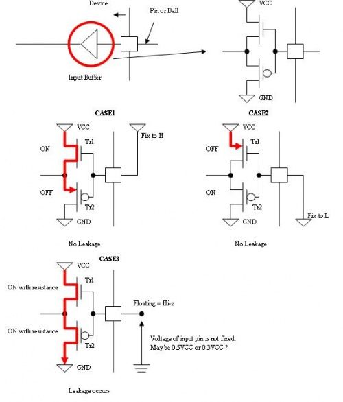
General CMOS input buffer consists of two transistors between VCC and GND. When input buffer is driven with fixed level (H or L), one transistor is ON and another transistor is OFF. In this case, there is no leakage since either of transistors is OFF and current between VCC and GND is shut. When input pin is floating, voltage level of this pin is not fixed. Sometime, it may be 0.5VCC, 0.3VCC. In this case, both transistors will be ON with resistance. This is mechanism of leakage by input pin floating. Please refer to Figure 1.
Figure 1. Input buffer leakage.
Bi-directional pin case
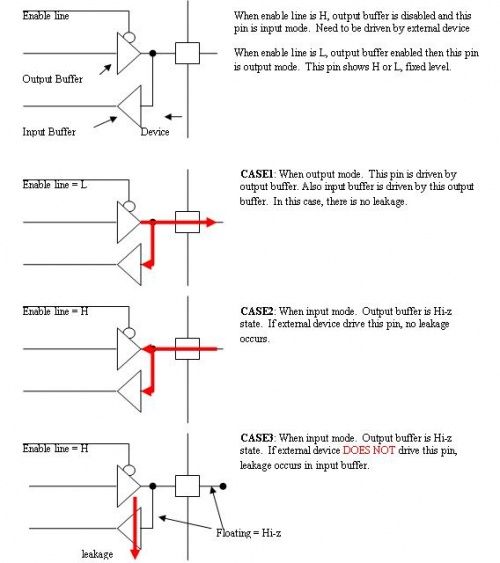
Basically, bi-directional pin consists of two buffers, output buffer and input buffer. General output buffer has enable line to drive output line. The enable line is controlled by internal logic and this is quit dependent on device specification. When output mode, this pin is driven by output buffer and fixed level is on the line. When the pin is input mode, external device should drive the pin. When the pin is input mode and floating, leakage current occurs. Please refer to Figure 2.
Figure 2. Bidirectional buffer leakage.
Internal pull-up/down case
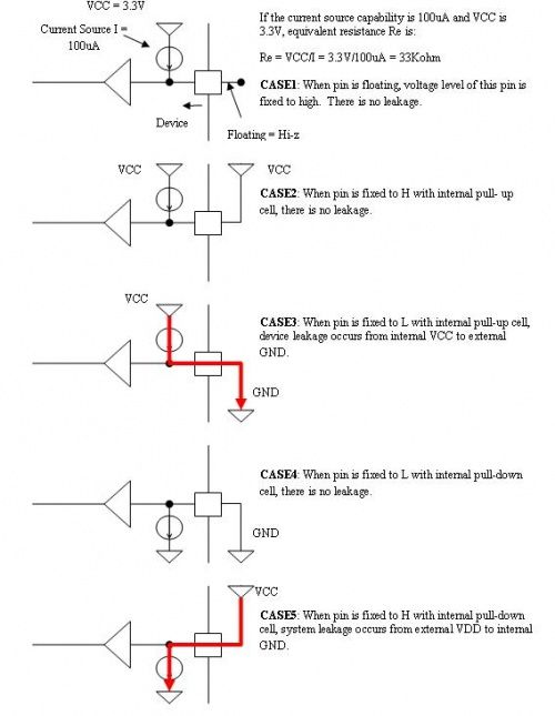
TI’ standard pull-up/down cell is current source, not actual resistance. This current source fixes voltage level when pin is floating. When pin with pull-up cell is tied to H, there is no current flow. But when this pin is fixed to L, device leakage occurs. See Figure - 3 CASE3. Also when the pin with pull-down cell is fixed to H, system leakage occurs. This is not device leakage. Refer to Figure - 3 CASE5.
Figure 3. Internal pull-up/down cell.
DM3xx Case Study
EMIF data bus (ARM_D[15:0])
EMIF data bus is made up of bi-directional pins. These should be configured as inputs when there is no access to EMIF. Pull-ups/downs are required. See Figure 4.
Figure 4. EMIF data bus case.

GIO case
GIO is bi-directional and input mode after reset. Most of case, pull-up or down resistor is required on GIO. Only one case, pull-up or down resister is not required. See Figure - 5.
Figure 5. GIO case.

ARM_A / EM_CE / EM_OE / EM_WE case
These signals are bi-directional signals. IO configuration of these signals depends on EXTHOST (external pin) and EMREL bit (0x30A1A:0). EMREL bit controls enable line of output buffer. When EMREL = 1, output buffer is disabled and input buffer is floating. See Figure 2. Default (after reset) value of EMREL = 0. Table - 1 shows IO configuration for these signals. Requirement of pull-up/down resistor is same as GIO case. See Figure 5.
Table 1: IO configuration for ARM_A / EM_CE / EM_OE / EM_WE
| EXTHOST | EMREL | IO |
| 0 | 0 | Output |
| 0 | 1 | Input (Hi-Z) |
| 1 | 0 | Input |
| 1 | 1 | Input (NA) |
EM_WAIT case
EM_WAIT is bi-directional signal. IO configuration of EM_WAIT is depending on EXTHOST (external pin) and WAITEN (0x0002:0). WAITEN bit controls enable line of output buffer. WAITEN = 0, output buffer is disabled and input buffer is floating. See Figure 2. Default value of WAIEN bit is 0. Table 2 shows IO configuration of EM_WAIT. Requirement of pull-up/down resistor is same as GIO case. See Figure 5.
Table 2: IO configuration of EM_WAIT
| EXTHOST | WAITEN | IO |
| 0 | 0 | Input |
| 0 | 1 | Input (NA) |
| 1 | 0 | Input (Hi-Z) |
| 1 | 1 | Output |
IO Power Optimization Guidelines from OMAP3530 TRM
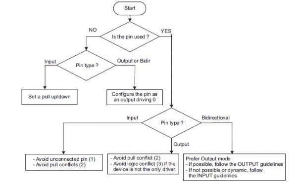
In order to optimize IO power, it is important to avoid unconnected or incorrectly-pulled pins.
Guidelines for avoiding extra current leakage:
- For input pins, use a pull up/down when possible.
- For output pins, check existing pulls to avoid conflicts.
- For bidirectional pins, reconfigure the pin as an output driving 0 when possible.
Figure 6. IO optimization flow chart.
The I/O pads are software-controlled by:
- Writing to the CONTROL.CONTROL_PADCONF_X registers in the Control Module for input/output and pull up/down configuration.
- Writing to the GPIOi.GPIO_OE registers in the GPIO module for input/output configuration.
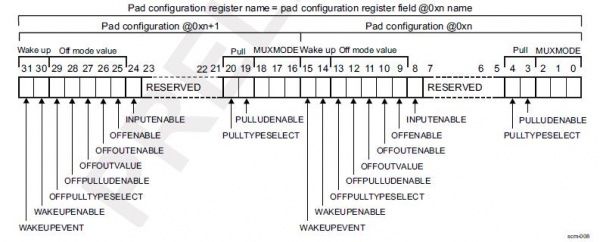
Figure 7. OMAP3530 Padconf register description .
For more information about how to configure the I/O pads, see the System Control Module chapter in the OMAP3530 Technical Reference Manual.
For more information about the GPIO module, see the General-Purpose Interface chapter in the OMAP3530 Technical Reference Manual.