《Digital Integrated Circuit》读后笔记 (三)
本文仅为个人娱乐分享,请勿用作其他用途
chapter six Static CMOS Design
- combinational logic
sequential logic a combinational logic portion and a module that holds the state
- Static CMOS Design
static complementary CMOS output is either V D D V_{DD} VDD or V S S V_{SS} VSS through a low-resistance path.
dynamic circuit class relies on temporary storage of signal values on the capacitance of high-impedance circuit nodes. simpler and faster sensitive to noise
- complementary CMOS
- ratioed logic(pseudo-NMOS and DCVSL)
- pass-transistor logic
- Complementary CMOS
pull-up network PUN PMOS
pull-down network PDN NMOS
series devices and parallel devices duality principle
N-input logic gate is 2N
sub-nets(SN)
Static properties: (Noise Margin)

- A=B=0->1: a strong pull-up
- A=1, B=0->1: V T n 1 = V t n 0 V_{Tn1}=V_{tn0} VTn1=Vtn0
- A=0->1, B=0: V T n 2 = V t n 0 + γ ( ( ∣ 2 ϕ T + V i n t ∣ − 2 ϕ T ) ) V_{Tn2}=V_{tn0}+\gamma((\sqrt{|2\phi_{T}+V_{int}|}-\sqrt{2\phi_{T}})) VTn2=Vtn0+γ((∣2ϕT+Vint∣−2ϕT))
Propagation Delay:
depends upon the input patterns
t p L H = 0.69 R p C L t_{pLH}=0.69R_pC_L tpLH=0.69RpCL
t p H L = 0.69 ( 2 R N C L ) t_{pHL}=0.69(2R_NC_L) tpHL=0.69(2RNCL)
To make the same delay, NMOS devices must be made twice as wide. PMOS remain unchanged.
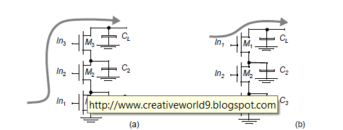
High-to-low propagation delay depends on the state of the internal nodes.
PMOS devices have a lower mobility relative to NMOS devices, stacking devices in series must be avoided as much as possible.
NAND is better than NOR.
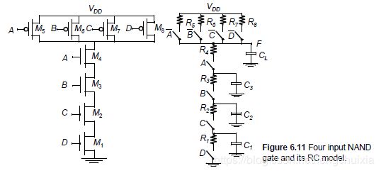
t p H L = 0.69 ( R 1 C 1 + ( R 1 + R 2 ) C 2 + ( R 1 + R 2 + R 3 ) C 3 + ( R 1 + R 2 + R 3 + R 4 ) C L ) t_{pHL}=0.69(R_1C_1+(R_1+R_2)C_2+(R_1+R_2+R_3)C_3+(R_1+R_2+R_3+R_4)C_L) tpHL=0.69(R1C1+(R1+R2)C2+(R1+R2+R3)C3+(R1+R2+R3+R4)CL)
= 0.69 R N ( C 1 + 2 C 2 + 3 C 3 + 4 C L ) =0.69R_N(C_1+2C_2+3C_3+4C_L) =0.69RN(C1+2C2+3C3+4CL)
Conclusion:
- Significant implementation area. 2N gate
- propagation delay is a function of the fan-in.
- t p = a 1 F I + a 2 F I 2 + a 3 F O t_p=a_1FI+a_2FI^2+a_3FO tp=a1FI+a2FI2+a3FO
Solution:
-
Transistor Sizing be used with caution
-
Progressive Transistor Sizing: M 1 > M 2 > M 3 > M 4 M_1>M_2>M_3>M_4 M1>M2>M3>M4 not simple in a real layout
-
Input Re-Ordering: critical path
-
Logic Restructuring
t p = t p 0 ( 1 + C e x t γ C g ) = t p 0 ( 1 + f / γ ) t_p=t_{p0}(1+\frac{C_{ext}}{\gamma C_{g}})=t_{p0}(1+f/\gamma) tp=tp0(1+γCgCext)=tp0(1+f/γ)
Modify: t p = t p 0 ( p + g f / γ ) t_p=t_{p0}(p+gf/\gamma) tp=tp0(p+gf/γ)
f f f :electrical effort
p p p: the ratio of the intrinstic delays of the complex gate and the simple inverter
g g g: logic effort
h h h: gate effort
Make t p t_p tp minimal: f 1 g 1 = f 2 g 2 = f 3 g 3 = . . . = f N g N f_1g_1=f_2g_2=f_3g_3=...=f_Ng_N f1g1=f2g2=f3g3=...=fNgN
F = f 1 f 2 f 3 f 4 . . f N = C L / C g 1 F=f_1f_2f_3f_4..f_N=C_L/C_{g1} F=f1f2f3f4..fN=CL/Cg1 G = g 1 g 2 . . . g N G=g_1g_2...g_N G=g1g2...gN H = F G H=FG H=FG
h = F G N = H N h=\sqrt[N]{FG} = \sqrt[N]{H} h=NFG=NH
Power Consumption:
dynamic power dissipation: α 0 − > 1 C L V D D 2 f \alpha_{0->1}C_LV_{DD}^{2}f α0−>1CLVDD2f switching activity
Logic function: α 0 − > 1 = p 0 p 1 = p 0 ( 1 − p 0 ) \alpha_{0->1}=p_{0}p_{1}=p_{0}(1-p_{0}) α0−>1=p0p1=p0(1−p0)
Assuming the inputs are independent and uniformly distributed
α 0 − > 1 = N 0 2 N N 1 2 N \alpha_{0->1}=\frac{N_{0}}{2^{N}}\frac{N_{1}}{2^{N}} α0−>1=2NN02NN1
- a conditional probability
- glitches/dynamic hazards long chains of gates
Solutions: To reduce the switching factor
-
Logic Restructuring
- Chain structure
- Tree structure
-
Input ordering
postpone the introduction of signals with a high transition rate
-
Time-multiplexing resources
can minimize the implementation area. Very few transitions
-
Glitch Reduction by balancing signal paths
Make every gate change simultaneously Redesigning the network
- Ratioed Logic

reduce robustness and extra power dissipation reduce number of gates N + 1 N+1 N+1
pseudo-NMOS gate nominal low output is not 0V
ratioed: voltage swing on the output and the overall functionality of the gate depends upon the ratio between the NMOS and PMOS sizes.
V O L ≈ μ p W p μ n W n ∣ V D S A T ∣ V_{OL}\approx\frac{\mu_pW_p}{\mu_nW_n}|V_{DSAT}| VOL≈μnWnμpWp∣VDSAT∣ To make V O L V_{OL} VOL smaller, PMOS needs to be sized much smaller, however, it is bad to propagation delay.
static power: P l o w = V D D I l o w P_{low}=V_{DD}I_{low} Plow=VDDIlow
differential logic and positive feedback:
DCVSL differetial cascode voltage switch logic
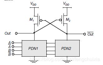
have rail-to-rail swing static power dissipation is eliminated
Of course, short circuit path still exists.
- Pass-transistor logic
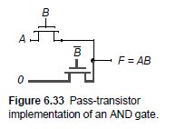
Reduced number of devices low capacitance
high output is V D D − V T n V_{DD}-V_{Tn} VDD−VTn low switching energy
pass-transistor gates cannot be cascaded by connecting the output of a pass gate to the gate input of another pass transistor.

may cosume static power when the output is high. insufficient to turn off the PMOS transistor of CMOS
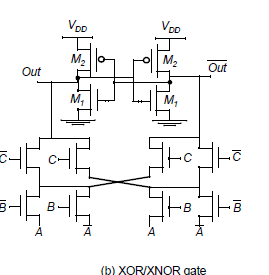
Differential Pass Transistor Logic:
CPL DPL
- complex gates such as XORs can be realized with a small number of transistors
- CPL is static gates
Solutions:
-
Level restoration:
level restorer

can eliminates any static power dissipation in the inverter.
the resistance of M n M_n Mn and M r M_r Mr must be such that the voltage at node X X X drops below the threshold of the inverter.
The rise time of the gate is further negatively affected, since, the level-restoring transistor M r M_r Mr fights the decrease in voltage at node X X X
swing-restored pass transistor logic
-
Multiple-threshold transistors:
zero-threshold transistor can make the subthreshold currents
-
Transmission gate logic:

NMOS devices pass a strong 0 but a weak 1, while PMOS transistor pass a strong 1 but a weak 0.
rail-to-rail swing
can realize multiplexer and XOR gate using less transistors.
R e q R_{eq} Req is relatively constant.

t p = 0.69 ∑ k = 0 n C R e q k = 0.69 C R e q n ( n + 1 ) 2 t_p=0.69\displaystyle \sum^{n}_{k=0}CR_{eq}k=0.69CR_{eq}\frac{n(n+1)}{2} tp=0.69k=0∑nCReqk=0.69CReq2n(n+1)
solution:
break the chain and insert buffers every n n n switches.
t p = 0.69 [ n m C R e q m ( m + 1 ) 2 ] + ( n m − 1 ) t b u f t_{p}=0.69[\frac{n}{m}CR_{eq}\frac{m(m+1)}{2}]+(\frac{n}{m}-1)t_{buf} tp=0.69[mnCReq2m(m+1)]+(mn−1)tbuf
m o p t = 1.7 t p b u f C R e q ≈ 3 m_{opt}=1.7\sqrt{\frac{t_{pbuf}}{CR_{eq}}}\approx3 mopt=1.7CReqtpbuf≈3
- Dynamic CMOS Design
to avoid the static power dissipation
precharge and evaluation phases determined by the signal C L K CLK CLK.
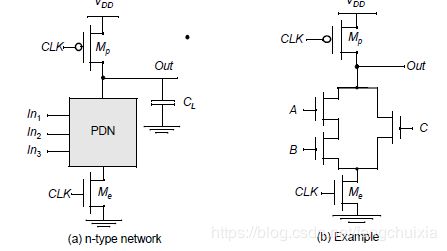
C L K = 1 CLK=1 CLK=1: evaluation phase
C L K = 0 CLK=0 CLK=0: precharge phase
During evaluation phase, the output can make at most one transition.
-
number of transistors: N + 2 N+2 N+2 numbers
-
non-ratioed
-
only consumes dynamic power
-
faster switching speeds
Speed and Power dissipation of dynamic logic
- t p L H = 0 t_{pLH}=0 tpLH=0
- no glitches only one transition
- a higher switching activity: α 0 − > 1 = p 0 \alpha_{0->1}=p_0 α0−>1=p0
Problems:
- charge leakage:

Source 1 and 2: reverse-biased diode and sub-threshold leakage
require a minimal clock rate
solution: adding a bleeder transistor

-
charge sharing:
share capacitor C L C_{L} CL and C a C_{a} Ca
we need to keep the value of Δ V o u t \Delta V_{out} ΔVout below ∣ V t p ∣ |V_{tp}| ∣Vtp∣
solution:
precharge critical internal nodes
-
Capacitive coupling:
back-gate coupling
example: a dynamic two-input NAND gate drives a static NAND gate
-
clock-feedthrough:
causes the output of the dynamic node to rise above V D D V_{DD} VDD on the low-to-high transition of the clock.
may cause forward-biased.


Cascading Dynamic gates:
the inputs can only make a single 0->1 transition during the evaluation period.
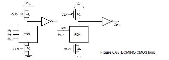
Domino Logic:
consist of an n-type dynamic logic block followed by a static inverter.
-
pure Domino design has become rare.
-
high speed only a rising edge delay exists.
Dual-rail Domino
n p np np-CMOS
