Xilinx SelectIO:个人整理
详细了解FPGA selectIO是学习FPGA基础,FPGA IO接口标准约束了IO的实现方式。大的分类:单端信号:LVCOMS、LVTTL;差分信号:SSTL、HCTL、LVDS、CML等,注意IO bank的VREF使用
Ø IOB
Ø IDELAY2
Ø ILOGIC2/ISERDES2
Ø ODELAY3
Ø OLOGIC/OSERDES3
Ø IO_FIFO
1. All VCCO pins for a given I/Obank must be connected to the same external voltage supply on the board, and asa result all of the I/O within a given I/O bank must share the same VCCO level.In HR I/O banks, if the I/O standard voltage requirement is < 1.8V, but aVCCO > 2.5V is applied , the device automatically enters an overvoltageprotection mode. Reconfiguring the device with the correct VCCO level restoresnormal operation.
2. VREF:Single-endedI/O standards with a differential input buffer require an input reference voltage(VREF). When VREF is required within an I/O bank, the two multi-function VREF pinsfor the bank must be used as VREF supply inputs. 7 series FPGAs can optionallyuse an internally generated reference voltage by enabling the INTERNAL_VREFconstraint。
3. To implement DCI in a design:
1. Assign one of the DCI I/O standards in an HP I/O bank (see Table1-2 and Table 1-3).
2. Connect the VRN multi-function pin to a precision resistor tiedto the VCCO rail for the
same bank.
3. Connect the VRP multi-function pin to a precision resistor tiedto ground.
4. Only one set of VRN and VRPresistors is used for each bank, so all DCI standards within each bank must beable to share the same external resistance values.
5. DCI Cascading:With DCIcascading, one I/O bank (the master bank) must have its VRN/VRP pins connectedto external reference resistors. Other I/O banks in the same HP I/O bank column(slave banks) can use DCI standards with the same impedance as the master bank,without connecting the VRN/VRP pins on these slave banks to external resistors.DCI impedance control in cascaded banks is received from the I/O master bank.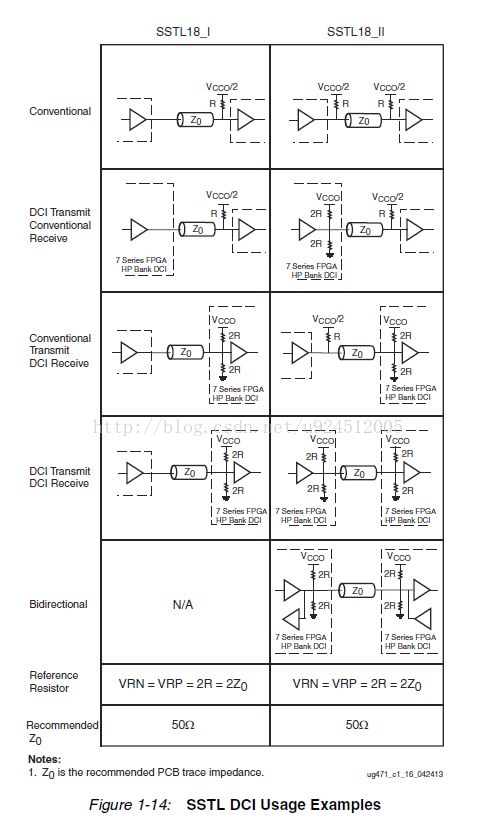
10. SSTL18 is is used for DDR2SDRAM memory interfaces. SSTL15 is used for DDR3 SDRAM memory interfaces. SSTL135is used for DDR3L SDRAM memory interfaces. SSTL12 supports Micron'snext-generation RLDRAM3 memory. The HSUL_12 standard is for LPDDR2 memorybuses.
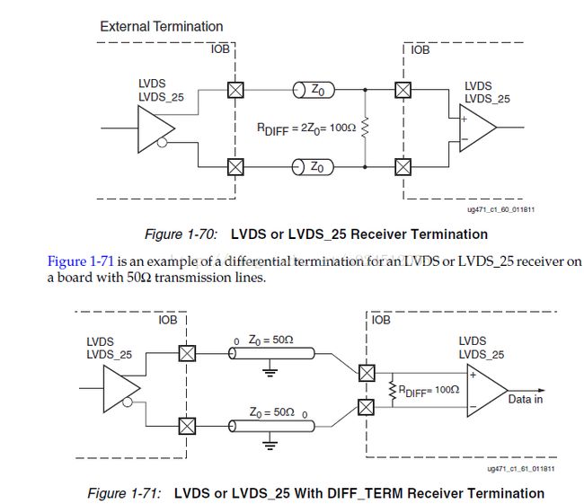
The 7series FPGA LVDS transmitter does not require any external termination. Table1-44 lists the allowed attributes corresponding to the 7 series FPGA LVDScurrent-mode drivers. 7 series FPGA LVDS current-mode drivers are a true currentsource and produce the proper (EIA/TIA compliant) LVDS signal. differentialtermination for an LVDS or LVDS_25 receiver on a board with 50Ω transmissionlines.
15.
16. Rules for Combining I/OStandards in the Same Bank:
1) Combining output standardsonly. Output standards with the same output VCCO requirement can be combined inthe same bank.
2) Combining input standards only.Input standards with the same VCCO and VREF requirements can be combined in thesame bank.
3) Combining input standards andoutput standards. Input standards and output standards with the same VCCOrequirement can be combined in the same bank.
4) Combining bidirectionalstandards with input or output standards. When combining bidirectional I/O withother standards, make sure the bidirectional standard can meet the first threerules.
17. ILOGIC Resources
18.
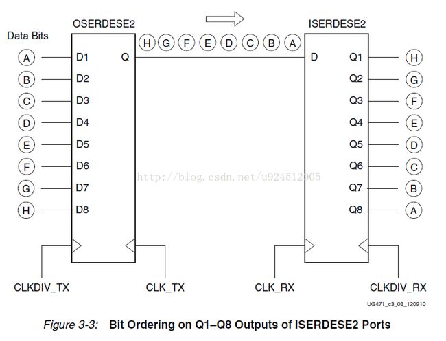
19. The ISERDESE2 deserializerenables high-speed data transfer without requiring the FPGA fabric to match theinput data frequency. This converter supports both single data rate (SDR) anddouble data rate (DDR) modes. In SDR mode, the serial-to-parallel convertercreates a 2-, 3-, 4-, 5-, 6-, 7-, or 8-bit wide parallel word. In DDR mode, theserial-to-parallel converter creates a 4-, 6-, 8-bit wide parallel word modewhen using one ISERDESE2, and 10- or 14-bit-wide parallel word when using twocascaded ISERDESE2.
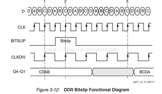
22. Bitslip Operation: In SDR mode,every Bitslip operation causes the output pattern to shift left by one. In DDRmode, every Bitslip operation causes the output pattern to alternate between ashift right by one and shift left by three. In this example, on the eighthBitslip operation,the output pattern reverts to the initial pattern. Thisassumes that serial data is an eight bit repeating pattern.
26. For external data flowing intothe FPGA, an IN_FIFO can connect to the ILOGIC (e.g., ISERDESE2, IDDR, or IBUF)to receive incoming data and pass it on to the fabric. For data flowing out ofthe FPGA, an OUT_FIFO can connect to the OLOGIC (e.g., OSERDESE2, ODDR, orOBUF) to pass data from the fabric and send it through to the IOB.
An IN_FIFO receives 4-bit data from an ILOGIC block while the fabricside reads either 4- or 8- bit data out of the array. An OUT_FIFO receives 4-or 8- bit data from the fabric while
an OLOGIC blockreads 4-bit data out of the array.
EachIO_FIFO has a 768-bit storage array and can be arranged as twelve groups of4-bit data or ten groups of 8-bit data. An IO_FIFO is nine entries deep,including an input and output register. Typical IO_FIFO uses are as a bufferfor a parallel I/O interface crossing between two frequency domains (e.g., theBUFR domain to/from the BUFG or BUFH domain) or as a 2:1serializer/deserializer to decouple the PHY from the fabric to relax fabricperformance requirements.


