1. 本次以三兄弟的DSP28335开发板为例,看下JTAG接口,EMU0,EMU1的用途,不是很懂,不深入研究,用到再说
EMU0/1是TI芯片的JTAG才有的信号,本身不属于JTAG标准里的信号,有两个作用。
(1)设定芯片是仿真模式(上拉)还是边界扫描模式(下拉)。
(2)用做高速实时数据交换RTDX及TRACE等功能时。这个一般用户可能用不到。
所以这两个信号是双向的,这个信号一般来说不需加要buffer,直接连起来就好了,不用管他是单向还是双向。

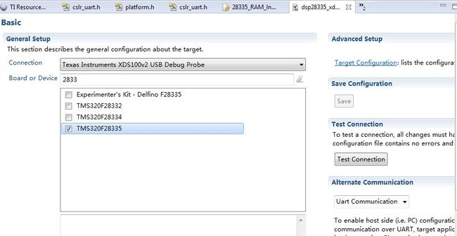
2. 打开工程,E:\dsp\SXD_C28335\SXD28335_PRO_1_V2\Example_2833x_LEDBlink,建立一个CCXML文件,编译一下工程
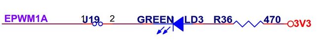
3. 看下引脚原理图,28335有3组GPIO,每组GPIO最多有32个引脚,但是28335是16位的,所以每组GPIO有高低寄存器
4. GPIO寄存器

5. 代码研究一下,看了一下底层用的是C2000WARE里面的库函数。
  1 #include "DSP28x_Project.h"     // Device Headerfile and Examples Include File
  2
  3 // Prototype statements for functions found within this file.
  4 interrupt void cpu_timer0_isr(void);
  5
  6 void main(void)
  7 {
  8
  9 // Step 1. Initialize System Control:
 10 // PLL, WatchDog, enable Peripheral Clocks
 11 // This example function is found in the DSP2833x_SysCtrl.c file.
 12    InitSysCtrl();
 13
 14 // Step 2. Initalize GPIO:
 15 // This example function is found in the DSP2833x_Gpio.c file and
 16 // illustrates how to set the GPIO to it's default state.
 17 // InitGpio();  // Skipped for this example
 18
 19
 20 // Step 3. Clear all interrupts and initialize PIE vector table:
 21 // Disable CPU interrupts
 22    DINT;
 23
 24 // Initialize the PIE control registers to their default state.
 25 // The default state is all PIE interrupts disabled and flags
 26 // are cleared.
 27 // This function is found in the DSP2833x_PieCtrl.c file.
 28    InitPieCtrl();
 29
 30 // Disable CPU interrupts and clear all CPU interrupt flags:
 31    IER = 0x0000;
 32    IFR = 0x0000;
 33
 34 // Initialize the PIE vector table with pointers to the shell Interrupt
 35 // Service Routines (ISR).
 36 // This will populate the entire table, even if the interrupt
 37 // is not used in this example.  This is useful for debug purposes.
 38 // The shell ISR routines are found in DSP2833x_DefaultIsr.c.
 39 // This function is found in DSP2833x_PieVect.c.
 40    InitPieVectTable();
 41
 42 // Interrupts that are used in this example are re-mapped to
 43 // ISR functions found within this file.
 44    EALLOW;  // This is needed to write to EALLOW protected registers
 45    PieVectTable.TINT0 = &cpu_timer0_isr;
 46    EDIS;    // This is needed to disable write to EALLOW protected registers
 47
 48 // Step 4. Initialize the Device Peripheral. This function can be
 49 //         found in DSP2833x_CpuTimers.c
 50    InitCpuTimers();   // For this example, only initialize the Cpu Timers
 51 #if (CPU_FRQ_150MHZ)
 52 // Configure CPU-Timer 0 to interrupt every 500 milliseconds:
 53 // 150MHz CPU Freq, 50 millisecond Period (in uSeconds)
 54    ConfigCpuTimer(&CpuTimer0, 150, 500000);
 55 #endif
 56 #if (CPU_FRQ_100MHZ)
 57 // Configure CPU-Timer 0 to interrupt every 500 milliseconds:
 58 // 100MHz CPU Freq, 50 millisecond Period (in uSeconds)
 59    ConfigCpuTimer(&CpuTimer0, 100, 500000);
 60 #endif
 61
 62 // To ensure precise timing, use write-only instructions to write to the entire register. Therefore, if any
 63 // of the configuration bits are changed in ConfigCpuTimer and InitCpuTimers (in DSP2833x_CpuTimers.h), the
 64 // below settings must also be updated.
 65
 66    CpuTimer0Regs.TCR.all = 0x4001; // Use write-only instruction to set TSS bit = 0
 67
 68 // Step 5. User specific code, enable interrupts:
 69
 70 // Configure GPIO32 as a GPIO output pin
 71    EALLOW;
 72    GpioCtrlRegs.GPBMUX2.bit.GPIO53 = 0;
 73    GpioCtrlRegs.GPBDIR.bit.GPIO53 = 1;
 74    GpioCtrlRegs.GPAMUX1.bit.GPIO0 = 0;
 75    GpioCtrlRegs.GPADIR.bit.GPIO0 = 1;
 76    EDIS;
 77
 78 // Enable CPU INT1 which is connected to CPU-Timer 0:
 79    IER |= M_INT1;
 80
 81 // Enable TINT0 in the PIE: Group 1 interrupt 7
 82    PieCtrlRegs.PIEIER1.bit.INTx7 = 1;
 83
 84 // Enable global Interrupts and higher priority real-time debug events:
 85    EINT;   // Enable Global interrupt INTM
 86    ERTM;   // Enable Global realtime interrupt DBGM
 87
 88 // Step 6. IDLE loop. Just sit and loop forever (optional):
 89    for(;;);
 90 }
 91
 92 interrupt void cpu_timer0_isr(void)
 93 {
 94    CpuTimer0.InterruptCount++;
 95    GpioDataRegs.GPBTOGGLE.all = 0x40000004; // Toggle GPIO32 once per 500 milliseconds
 96    GpioDataRegs.GPBTOGGLE.bit.GPIO53 = 1;
 97    GpioDataRegs.GPATOGGLE.bit.GPIO0 = 1;
 98    // Acknowledge this interrupt to receive more interrupts from group 1
 99    PieCtrlRegs.PIEACK.all = PIEACK_GROUP1;
100 }
6. 看下GPIO的全局变量volatile struct GPIO_CTRL_REGS GpioCtrlRegs;,volatile 确保本条指令不会被编译器优化,从下面看的出来,函数库将GPIOA,GPIOB,GPIOC,的控制寄存器全部写在一起了。数据寄存器也是一样的GpioDataRegs.GPATOGGLE.bit.GPIO0 = 1;
 1 struct GPIO_CTRL_REGS {
 2    union  GPACTRL_REG  GPACTRL;   // GPIO A Control Register (GPIO0 to 31)
 3    union  GPA1_REG     GPAQSEL1;  // GPIO A Qualifier Select 1 Register (GPIO0 to 15)
 4    union  GPA2_REG     GPAQSEL2;  // GPIO A Qualifier Select 2 Register (GPIO16 to 31)
 5    union  GPA1_REG     GPAMUX1;   // GPIO A Mux 1 Register (GPIO0 to 15)
 6    union  GPA2_REG     GPAMUX2;   // GPIO A Mux 2 Register (GPIO16 to 31)
 7    union  GPADAT_REG   GPADIR;    // GPIO A Direction Register (GPIO0 to 31)
 8    union  GPADAT_REG   GPAPUD;    // GPIO A Pull Up Disable Register (GPIO0 to 31)
 9    Uint32              rsvd1;
10    union  GPBCTRL_REG  GPBCTRL;   // GPIO B Control Register (GPIO32 to 63)
11    union  GPB1_REG     GPBQSEL1;  // GPIO B Qualifier Select 1 Register (GPIO32 to 47)
12    union  GPB2_REG     GPBQSEL2;  // GPIO B Qualifier Select 2 Register (GPIO48 to 63)
13    union  GPB1_REG     GPBMUX1;   // GPIO B Mux 1 Register (GPIO32 to 47)
14    union  GPB2_REG     GPBMUX2;   // GPIO B Mux 2 Register (GPIO48 to 63)
15    union  GPBDAT_REG   GPBDIR;    // GPIO B Direction Register (GPIO32 to 63)
16    union  GPBDAT_REG   GPBPUD;    // GPIO B Pull Up Disable Register (GPIO32 to 63)
17    Uint16              rsvd2[8];
18    union  GPC1_REG     GPCMUX1;   // GPIO C Mux 1 Register (GPIO64 to 79)
19    union  GPC2_REG     GPCMUX2;   // GPIO C Mux 2 Register (GPIO80 to 95)
20    union  GPCDAT_REG   GPCDIR;    // GPIO C Direction Register (GPIO64 to 95)
21    union  GPCDAT_REG   GPCPUD;    // GPIO C Pull Up Disable Register (GPIO64 to 95)
22 };
7. 还有一些汇编指令,以后再研究吧
1 #define  EINT   asm(" clrc INTM")
2 #define  DINT   asm(" setc INTM")
3 #define  ERTM   asm(" clrc DBGM")
4 #define  DRTM   asm(" setc DBGM")
5 #define  EALLOW asm(" EALLOW")
6 #define  EDIS   asm(" EDIS")
7 #define  ESTOP0 asm(" ESTOP0")