FET
文章目录
- How FET got its Name
- JFET (Junction FET)
- I-V Characteristics
- Questions
- Pinch-off voltage
- Channel Current
- Gain (Transconductance)
- MESFET (Metal Semiconductor FET)
- Metal-Semiconductor (MS) Contact
- Schottky Diode
- Heavily Doped (Degenerately Doped) Semiconductor
- Schottky Diode Calculations
- MOSFET (Metal-Oxide FET)
- Composition
- Terminal Naming
- Functionality (NMOS)
- MOS Energy Band Diagram
- MOS Calculations
- Φ S \Phi_S ΦS: Surface Potential
- Φ F \Phi_F ΦF
- Depletion Width W W W
- Threshold Voltage V T V_T VT
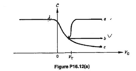
- Cap-Voltage Characteristics
- Supplement
- JFET pinch-off
- Why doesn't current goto 0
- How does current flow after pinch-off
- Gradual Channel Approx
- JFET Transconductance
- JFET Transconductance
- How FET got its Name
- JFET (Junction FET)
- I-V Characteristics
- Questions
- Pinch-off voltage
- Channel Current
- Gain (Transconductance)
- I-V Characteristics
- MESFET (Metal Semiconductor FET)
- Metal-Semiconductor (MS) Contact
- Schottky Diode
- Heavily Doped (Degenerately Doped) Semiconductor
- Schottky Diode Calculations
- MOSFET (Metal-Oxide FET)
- Composition
- Terminal Naming
- Functionality (NMOS)
- MOS Energy Band Diagram
- MOS Calculations
- KaTeX parse error: Undefined control sequence: \PhiS at position 1: \̲P̲h̲i̲S̲: Surface Potential
- KaTeX parse error: Undefined control sequence: \PhiF at position 1: \̲P̲h̲i̲F̲
- Depletion Width W W W
- Threshold Voltage V T VT VT
- Cap-Voltage Characteristics
- Supplement
- JFET pinch-off
- Why doesn’t current goto 0
- How does current flow after pinch-off
- Gradual Channel Approx
- JFET Transconductance
How FET got its Name
A voltage applied to the metallic plate modalated the conductance of the underlying semiconductor, which in turn modulated the carrent flowing between ohmic contacts A and B. This phenomenon, where the conductivity of a semiconductor is modulated by an electric field applied normal to the surface of the semiconductor, has been named the field effect.
JFET (Junction FET)

Suppose we connect S to ground, reverse bias at S is V G V_G VG.
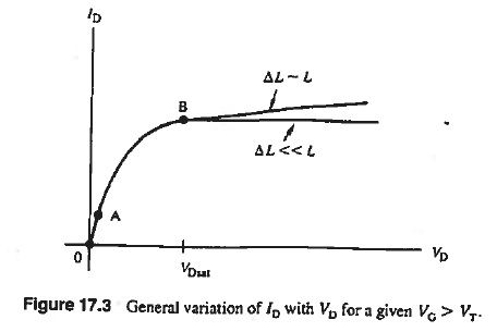
I-V Characteristics
- V G V_G VG = 0. When VD is small, ID is small. Linear I-V. No change in depletion width across channel.

- V G V_G VG increases. Channel pinches-off.


Questions
- Should/Should not I D I_D ID = 0 beyond pinch-off?
No. Carriers can also pass depletion region, but see a much higher resisitance. - Why does V D V_D VD > V D S a t V_D^{Sat} VDSat have no effect on ID?
Increasing V D V_D VD will also increase the length of pinched-off region. These two effects cancel out.
Pinch-off voltage
V p V_p Vp = Reverse bias between n-channel and p + p^+ p+ gate at the drain end ( x = 0 ) (x=0) (x=0).
h ( x ) h(x) h(x) = Channel half-width at any x x x
a a a = half width of channel
Assumptions:
- Channel with at x = 0 x=0 x=0 decreases uniformly as the reverse bias increases to pinch-off.
- V b i V_{bi} Vbi neglected.
- p + − n p^+-n p+−n gate junction.
V p = q a 2 N D 2 ε V_p=\frac{qa^2N_D}{2\varepsilon} Vp=2εqa2ND
a a a: half thickness
Channel Current
L L L: length
Z Z Z: depth
2 a 2a 2a: thickness
I D = G o V P [ V D V P + 2 3 ( − V G V P ) 3 / 2 − 2 3 ( V D − V G V P ) 3 / 2 ] I_D=G_oV_P\left[\frac{V_D}{V_P} + \frac23\left(-\frac{V_G}{V_P}\right)^{3/2} - \frac23\left(\frac{V_D-V_G}{V_P}\right)^{3/2}\right] ID=GoVP[VPVD+32(−VPVG)3/2−32(VPVD−VG)3/2]
G o = 2 a Z ρ L G_o=\frac{2aZ}{\rho L} Go=ρL2aZ
I D ( s a t ) = G o V P [ V D V P + 2 3 ( − V G V P ) 3 / 2 − 2 3 ] I_D(sat)=G_oV_P\left[\frac{V_D}{V_P} + \frac23\left(-\frac{V_G}{V_P}\right)^{3/2} - \frac23\right] ID(sat)=GoVP[VPVD+32(−VPVG)3/2−32]
Gain (Transconductance)
g m ( s a t ) = ∂ I D ( s a t ) ∂ V G = G o [ 1 − ( − V G V P ) 1 / 2 ] g_m(sat)=\frac{\partial I_D(sat)}{\partial V_G}=G_o\left[1-\left(-\frac{V_G}{V_P}\right)^{1/2}\right] gm(sat)=∂VG∂ID(sat)=Go[1−(−VPVG)1/2]
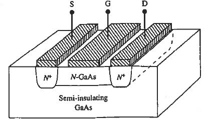
MESFET (Metal Semiconductor FET)
Metal-Semiconductor (MS) Contact
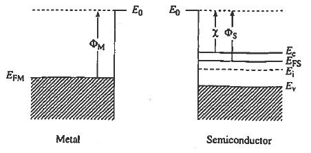
- Φ M \Phi_M ΦM: Metal Work Function (the one in photoelectric effect)
- Φ S \Phi_S ΦS: Semiconductor Work Function
- χ \chi χ: Electron Affinity. χ = ( E 0 − E C ) ∣ s u r f a c e \chi=(E_0-E_C)|_{surface} χ=(E0−EC)∣surface
Φ S = χ + ( E c − E F ) F B \Phi_S=\chi+(E_c-E_F)_{FB} ΦS=χ+(Ec−EF)FB
- ( E c − E F ) F B (E_c-E_F)_{FB} (Ec−EF)FB: Energy difference between E c E_c Ec and E F E_F EF at flat band (i.e.) zero bias condition.

Φ B = Φ M − χ \Phi_B=\Phi_M-\chi ΦB=ΦM−χ
- Φ B \Phi_B ΦB: surface potential-energy barrier encountered by electrons with E = E F E=E_F E=EF in the metal.
Schottky Diode
- Φ M > Φ S \Phi_M>\Phi_S ΦM>ΦS: Applying V A > 0 V_A>0 VA>0 lowers E F M E_{FM} EFM below E F S E_{FS} EFS, reduces the barrier seen by electrons in the semiconductor.

- Φ M < Φ S \Phi_M<\Phi_S ΦM<ΦS: Non-rectifying, Ohmic.

Heavily Doped (Degenerately Doped) Semiconductor

When the barrier is thin enough, the carriers can tunnel through.
Upper: forward bias. Below: rev bias
Additional component of current
Schottky Diode Calculations
- Built-in Voltage
V b i = 1 q [ Φ B − ( E c − E F ) F B ] V_{bi}=\frac1q\left[\Phi_B-(E_c-E_F)_{FB}\right] Vbi=q1[ΦB−(Ec−EF)FB]
- ρ \rho ρ
- Metal: delta function (charge only on surface)
- Semiconductor: ρ = q N D \rho=qN_D ρ=qND
- E E E:
E ( x ) = − q N D ε S i ( W − x ) … 0 ≤ x ≤ W E(x)=-\frac{qN_D}{\varepsilon_{Si}}(W-x)\ldots 0\le x\le W E(x)=−εSiqND(W−x)…0≤x≤W
- V V V:
V ( x ) = − q N D 2 ε S i ( W − x ) 2 … 0 ≤ x ≤ W V(x)=-\frac{qN_D}{2\varepsilon_{Si}}(W-x)^2\ldots 0\le x \le W V(x)=−2εSiqND(W−x)2…0≤x≤W
- Depletion Width
W = 2 ε S i q N D ( V b i − V A ) W=\sqrt{\frac{2\varepsilon_{Si}}{qN_D}(V_{bi}-V_A)} W=qND2εSi(Vbi−VA)
- Φ ( x ) \Phi(x) Φ(x)
Φ ( x ) = q N D x 2 2 ϵ S \Phi(x)=\frac{qN_Dx^2}{2\epsilon_S} Φ(x)=2ϵSqNDx2
- Current Density
J = J S ( e q V a / k T − 1 ) J=J_S(e^{qV_a/kT}-1) J=JS(eqVa/kT−1)
J S = A ∗ T 2 exp ( − q Φ B k T ) J_S=A^*T^2\exp\left(-\frac{q\Phi_B}{kT}\right) JS=A∗T2exp(−kTqΦB)
A ∗ A^* A∗ is the Effective Richardson Constant
MOSFET (Metal-Oxide FET)
Composition
- MOS Capacitor
- Two pn juncitons
Terminal Naming
- Carriers enter the structure through Source (S)
- Leave through the Drain (D)
- Subject to the control of the Gate (G)
Functionality (NMOS)
- When V G ≤ V T V_G\le V_T VG≤VT, i.e. V G V_G VG is in accumulation or depletion biased, the gated region contains mostly holes and few electrons, an open circuit is formed.
- When V G > V T V_G>V_T VG>VT, i.e. V G V_G VG is inversion biased, an inversion layer (channel) containing mobile electrons is formed.
- As V D V_D VD increases, the channel finally pinches-off, the current saturates.

MOS Energy Band Diagram

- Accumulation ( V G < 0 V_G<0 VG<0) holes accumulate on the semiconductor side of the gate
- Depletion ( 0 < V G < V T 0
- Inversion ( V G > V T V_G>V_T VG>VT) electron density increase
- Initially, n < n i n
n<ni . - n = n i n=n_i n=ni when E i = E F E_i=E_F Ei=EF
- Initially, n < n i n
- When V G = V T V_G=V_T VG=VT, n = N A n=N_A n=NA, the semiconductor seems no longer to be depleted. Instead, it now behave similar to n-type. The channel has formed.
MOS Calculations
Φ S \Phi_S ΦS: Surface Potential
Φ S = 1 q [ E i ( b u l k ) − E i ( s u r f a c e ) ] \Phi_S=\frac1q[E_i(bulk)-E_i(surface)] ΦS=q1[Ei(bulk)−Ei(surface)]
Φ F \Phi_F ΦF
Φ F = 1 q [ E i ( b u l k ) − E F ] \Phi_F=\frac1q[E_i(bulk)-E_F] ΦF=q1[Ei(bulk)−EF]
In p-type, N A ≫ N D N_A\gg N_D NA≫ND, p b u l k = n i exp ( [ E i ( b u l k ) − E F ] / k T ) = N A p_{bulk}=n_i\exp([E_i(bulk)-E_F]/kT)= N_A pbulk=niexp([Ei(bulk)−EF]/kT)=NA
Φ F = k T q ln ( N A n i ) \Phi_F=\frac{kT}{q}\ln\left(\frac{N_A}{n_i}\right) ΦF=qkTln(niNA)
In n-type, N D ≫ N A N_D\gg N_A ND≫NA, n b u l k = n i exp ( [ E F − E i ( b u l k ) ] ) = N D n_{bulk}=n_i\exp([E_F-E_i(bulk)])=N_D nbulk=niexp([EF−Ei(bulk)])=ND
Φ F = − k T q ln ( N D n i ) \Phi_F=-\frac{kT}{q}\ln\left(\frac{N_D}{n_i}\right) ΦF=−qkTln(niND)
When V G = V T V_G=V_T VG=VT,
Φ S = 2 Φ F \Phi_S=2\Phi_F ΦS=2ΦF
Depletion Width W W W
Valid before strong inversion:
W = 2 ε S i q N A Φ S W=\sqrt{\frac{2\varepsilon_{Si}}{qN_A}\Phi_S} W=qNA2εSiΦS
At strong inversion:W m = 2 ϵ k T q 2 N A ln ( N A n i ) W_m=2\sqrt{\frac{\epsilon kT}{q^2N_A}\ln\left(\frac{N_A}{n_i}\right)} Wm=2q2NAϵkTln(niNA)
When V G = V T V_G=V_T VG=VT, Φ S = 2 Φ F \Phi_S=2\Phi_F ΦS=2ΦF, the depletion width
W T = 4 ε S i q N A Φ F W_T=\sqrt{\frac{4\varepsilon_{Si}}{qN_A}\Phi_F} WT=qNA4εSiΦF
Threshold Voltage V T V_T VT
For N(-channel)MOS (P-bulk)
V T = 2 Φ F + ϵ O X I D E x O ϵ S i 4 q N A ϵ S i Φ F V_T=2\Phi_F+\frac{\epsilon_{OXIDE}x_O}{\epsilon_{Si}}\sqrt{\frac{4qN_A}{\epsilon_{Si}}\Phi_F} VT=2ΦF+ϵSiϵOXIDExOϵSi4qNAΦF
For PMOS (N-bulk)
V T = 2 Φ F − ϵ O X I D E x O ϵ S i 4 q N D ϵ S i ( − Φ F ) V_T=2\Phi_F-\frac{\epsilon_{OXIDE}x_O}{\epsilon_{Si}}\sqrt{\frac{4qN_D}{\epsilon_{Si}}(-\Phi_F)} VT=2ΦF−ϵSiϵOXIDExOϵSi4qND(−ΦF)
x O x_O xO is the thickness of the OXIDE
Cap-Voltage Characteristics

Supplement
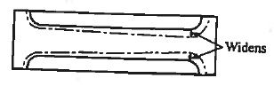
JFET pinch-off

Widening everywhere as V S D V_{SD} VSD grows
Why doesn’t current goto 0
If current is 0, the pinch-off will disappear. To maintain pinch-off, a non-zero current must be present.
How does current flow after pinch-off
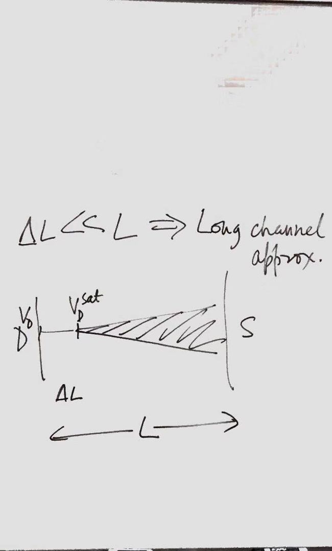
Gradual Channel Approx
Formula for depetion layer width remainis same at every point and edge of depletion layer is not a multi-valued function at any point
JFET Transconductance
g m = ∂ I D ( s a t ) ∂ V G g_m=\frac{\partial I_D(sat)}{\partial V_G} gm=∂VG∂ID(sat)
Proportional to V G \sqrt{V_G} VG
e at every point and edge of depletion layer is not a multi-valued function at any point
JFET Transconductance
g m = ∂ I D ( s a t ) ∂ V G g_m=\frac{\partial I_D(sat)}{\partial V_G} gm=∂VG∂ID(sat)
Proportional to V G \sqrt{V_G} VG