时钟偏差、延迟、不确定度、抖动 (skew,latency,uncertainty,jitter)
skew,latency,uncertainty,jitter
- Remark:physicaldesign4u
-
- Skew
- Types of clock skew
-
- Positive skew(利于setup time)
- Negative skew(利于Hold time)
- Zero skew
- Local skew
- Global skew
- Useful skew
- Latency
- Clock Uncertainty
-
- Static clock uncertainty
- Dynamic clock uncertainty
- Jitter
- The question of why the clock does bit always arrive exactly after one clock?为什么时钟总是在一个时钟之后精确到达的问题?
Remark:physicaldesign4u
Skew
This phenomenon in synchronous circuits(同步电路). The Difference in arrival of clock at two consecutive pins(连续引脚) of a sequential element.
我们把时钟信号到达不同寄存器的时间偏差称为skew。 一直以来,Skew都是衡量时钟树性能的重要参数,传统CTS的目的就是为了减小skew。

- Sources of skew:
- Wire interconnect length
- Capacitive loading mismatch
- Material imperfections(材料缺陷)
- Temperature variations
- Differences in input capacitance on the clock inputs
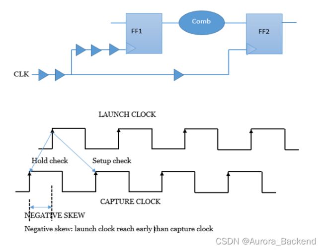
Types of clock skew
Positive skew(利于setup time)
- if the capture clock comes late than the launch clock.

Negative skew(利于Hold time)
- if the capture clock comes early than the launch clock.
Zero skew
- when the capture clock and launch clock arrives at the same time. (ideally, it is not possible)

Local skew
- difference in arrival of clock at two consecutive pins of sequential element.it can be positive and negative local skew also.

Global skew
-
the difference between max insertion delay and the min insertion delay.it can be positive and negative local skew also.
-
max insertion delay
delay of the clock signal takes to propagate to the farthest leaf cell in the design. -
min insertion delay
delay of the clock signal takes to propagate to the nearest leaf cell in the design.
Useful skew
- if the clock is skewed intentionally to resolve setup violations.

Latency
The delay difference from the clock generation point to the clock endpoints.
- ON-CHIP CLOCK SOURCE

- OFF CHIP CLOCK SOURCE

- There are two types of latency
- Source latency(时钟源插入延迟)
- Source latency is also called insertion delay. The delay from the
clock sourceto theclock definition points. Source latency could represent either on-chip or off-chip latency.
- Source latency is also called insertion delay. The delay from the
- Network latency
- The delay from the
clock definition points(create_clock) to theflip-flop clock pins.
- The delay from the
- Source latency(时钟源插入延迟)
- The total clock latency at the clock in a flip flop is the sum of the source and network latencies.
Set_clock_latency 0.8 [get_clocks clk_name1] ----> network latency
Set_clock_latency 1.9 –source [get_clocks clk_name1] -------> source latency
Set_clock_latency 0.851 –source –min [get_clocks clk_name2] -----> min source latency
Set_clock_latency 1.322 –source –max [get_clocks clk_name2] ------> max source latency
One important distinction to observe between source and network latency is that once a clock tree is built for the design, the network latency can be ignored. However the source latency remains even after the clock tree is built.
在时钟源插入延迟和时钟网络延迟之间需要注意的一个重要区别是,一旦构建了一个时钟树,时钟网络延迟network latency就可以被忽略。然而,即使在构建了时钟树之后,时钟源插入延迟source latency仍然存在。
The network latency is an estimate of the delay of the clock tree before clock tree synthesis. After clock tree synthesis, the total clock latency from the clock source to a clock in of a flip flop is the source latency plus **actual delay** of the clock tree from the clock definition point to the flip flop
network latency是时钟树综合之前对时钟树延迟的估计。时钟树综合后,从时钟源到触发器时钟引脚的时钟总延迟就是时钟源插入延迟加上从时钟定义点到触发器时钟树的实际延迟。
Clock Uncertainty
clock uncertainty is the difference between the arrivals of clocks at registers in one clock domain or between domains. it can be classified as static and dynamic clock uncertainties.
时钟不确定性是时钟沿的实际到达时间相对于理想到达时间的偏差。在理想模式下,时钟信号可以同时到达所有时钟引脚。
但事实上,完美是不可能实现的。而理想模式应该引入一些不确定的变量来模拟·真实的传播模式。“理想模式”下时钟假定时钟不确定。
时钟不确定性是时钟本身的不完美导致的。譬如对于100MHz时钟,上升沿本应该在0ns,10ns,20ns;实际上却在0ns,10.01ns,19.99ns,这个差距就是时钟的不确定性Clock Uncertaint·。
Timing Uncertainty of clock period is set by the command set_clock_uncertainty at the synthesis stage to reserve(预留) some part of the clock period for uncertain factors (like skew, jitter, OCV, CROSS TALK, MARGIN or any other pessimism) which will occur in PNR stage. The uncertainty can be used to model various factors that can reduce the clock period.
It can define for both setup and hold.
Set_clock_uncertainty –setup 0.2 [get_clocks clk_name1]

Set_clock_uncertainty –hold 0.05 [get_clocks clk_name1]
Clock uncertainty for setup effectively reduces the available clock period by the specified amount as shown in fig.
And the clock uncertainty for hold is used as an additional margin that needs to be satisfied.
在setup check中,clock uncertainty是代表着降低了时钟的有效周期;而在hold check中,clock uncertainty是代表着hold check所需要满足的额外margin。

- Pre CTS uncertainty = clock skew + jitter + margin
- CTS uncertainty = jitter + margin
- Clock uncertainty
- in the ideal mode we assume the clock is arriving at all the flip flop at the same time.But acaually, we did not get the clock at the same time, maybe the clock will arrive at different times at different clock pins of a flip flop. so in ideal mode clock assume some uncertainty .For example a 1ns clock with 100 ps clock uncertainty means that next clock pulse will occur after 1ns±50ps (either + or -).
Static clock uncertainty
it does not vary or varies very slowly with time. Process variation induced clock uncertainty. An example of this is clock skew.
- Sources of static clock uncertainty
- Intentional and unintentional mismatch in design
- On-chip variation (OCV)
- Load variation at every stage in clock distribution
Dynamic clock uncertainty
it varies with time. Dynamic power supply induced delay variation and clock jitter is the example of this
- Sources of dynamic clock uncertainty
- Voltage drop and dynamic voltage variations
- Temperature variations
- Clock generator jitter
Jitter
Jitter is the short term variations of a signal with respect to its ideal position in time. (相对于其理想位置在时间上的短期变化)
It is the variation of the clock period from edge to edge.it can vary +/- jitter value. From cycle to cycle the period and duty cycle can change slightly due to the clock generation circuitry. (由于时钟生成电路的不同,周期和占空比可能会因周期而略有变化。)
This can be modeled by adding uncertainty regions around the rising and falling edge of the clock waveform.
- Sources of jitter
- Internal circuitry of the PLL(锁相环的内部电路)
- Thermal noise in crystal oscillators(晶体振荡器中的热噪声)
- Transmitters and receivers of resonating devices(谐振器件)
The first important point is that there are two phases in the design of when we are using a clock signal. In the first stage i.e. during RTL design, during synthesis and during placement the clock is ideal. The ideal clock has no distribution tree, it is directly connected at the same time to all flip flop clock pins.(时钟处于“ideal理想模式”(例如:RTL设计期间、综合期间和布局期间)。)
The second phase comes when CTS inserts the clock buffer to build the clock tree into the design that carries the clock signal from the clock source pin to the all flip flops clock pins. After CTS is finished clock is called “propagated clock”.(第二阶段是时钟树综合(CTS)将实际的缓冲器树插入设计中,该树将时钟信号从时钟源引脚传送到触发器时钟引脚。CTS是在place之后和route之前完成的。CTS完成后,时钟被称为“propagation clock”。)
Clock latency term we are using when the clock is in ideal mode. It is the delay that exists from the clock source to the clock pin of the flip flop. This delay is specified by the user (not a real value or measured value).
When the clock is in propagated mode the actual delay comes into the picture then this delay is called as insertion delay. Insertion delay is a real and measured delay path through a tree of buffers. Sometimes the clock latency is interpreted as a desired target value for insertion delay.(时钟延迟被解释为插入延迟所需的目标值。)
The question of why the clock does bit always arrive exactly after one clock?为什么时钟总是在一个时钟之后精确到达的问题?
- The reasons are:
- The insertion delay to the launching flip flop’s clock pin is different than the insertion delay of capturing clock (like maybe
capture clock is coming before then the launch clock or capture clock is coming after the launch clockthat difference is calledskew) - The clock period is not constant. Some clock cycles may are longer or shorter than others in a random fashion. This is called
clock jitter.时钟周期不是恒定的。 一些时钟周期可能以随机方式比其他时钟周期更长或更短。 这称为时钟抖动。 - Even if the capture clock path and launch clock path are identical, may be their path delays are different, because different derate are applies on the path
Because the chip having different delay properties(延迟属性) across the die due toprocess voltage and temperature variationi.e. called OCV (on-chip variation). This essentially increases the clock skew.
- The insertion delay to the launching flip flop’s clock pin is different than the insertion delay of capturing clock (like maybe