《Digital Integrated Circuits》读后笔记(二)
本文仅作个人娱乐分享,请勿用作其他用途
chapter 5 The CMOS Inverter
- inverter gate
- cost
- static behavior
- dynamic response
- energy and power consumption
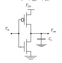
- The Static CMOS inverter
MOS: when ∣ V G S < V T ∣ |V_{GS}
when ∣ V G S > V T ∣ |V_{GS}>V_{T}| ∣VGS>VT∣ , the on-resistance is finite
Ideal Features:
-
when V i n V_{in} Vin is high, NMOS is on, PMOS is off. V o u t V_{out} Vout is 0.
when V i n V_{in} Vin is low, NMOS is off, PMOS is on. V o u t V_{out} Vout is V D D V_{DD} VDD.
Swing is from V D D V_{DD} VDD and G N D GND GND . logic level is not dependent upon the relative device sizes.
-
steady state: finite resistance between output and V D D V_{DD} VDD or G N D GND GND . No current flow, no static power.
-
input resistance is extremely high. Theoretically, inverter can have an infinite fan-out.
However, increasing fan-out will increase the propagation delay.
VTC(voltage-transfer characteristic):

a narrow transition zone.
Transient behavior:
output capacitance of the gate, C L C_L CL
composed of drain diffusion capacitances of NMOS and PMOS transistors, the capacitance of the connecting wires, the input capacitance of fan-out gates.
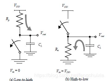
response time: time constant R p C L R_pC_L RpCL.
Conclusion: A fast gate is built by keeping the output capacitance small or by decreasing the on-resistance of the transistor.
Robustness: static CMOS converter is insensitive to these variations
- The switching threshold of CMOS inverter V M V_M VM
noise margin V I H V_{IH} VIH and V I L V_{IL} VIL
switching threshold V M V_M VM is defined as the point where V i n = V o u t V_{in} = V_{out} Vin=Vout.
Supposed the supply voltage is high and the velocity-saturated appear:
V M = r V D D 1 + r V_{M} = \frac{rV_{DD}}{1+r} VM=1+rrVDD ( V D D V_{DD} VDD is high) r = k p V D S A T p k n V D S A T n = υ s a t p W p υ s a t n W n r = \frac{k_pV_{DSATp}}{k_nV_{DSATn}} = \frac{\upsilon_{satp}W_p}{\upsilon_{satn}W_n} r=knVDSATnkpVDSATp=υsatnWnυsatpWp
if V M V_M VM located at mid, r = 1 r = 1 r=1, and ( W / L ) p = ( W / L ) n × ( V D S A T n k n ’ / V D S A T p k p ′ ) (W/L)_p = (W/L)_n\times (V_{DSATn}k_n^{’}/V_{DSATp}k_p^{'}) (W/L)p=(W/L)n×(VDSATnkn’/VDSATpkp′)
if V M V_M VM is required high, then r > 1 r>1 r>1, make PMOS wider
Analysis:
- V M V_M VM - W p / W n W_p/W_n Wp/Wn : V M V_M VM is insensitive to the ratio. So we can set the width of the PMOS transistor to values smaller than those required for symmetry.
- If required asymmetrical transfer characteristics, then we can change the ratio.
- Noise margin N M H NM_H NMHand N M L NM_L NML:
V I H V_{IH} VIH and V I L V_{IL} VIL :operational points of the inverter where d V o u t d V i n = − 1 \frac {dV_{out}}{dV_{in}} = -1 dVindVout=−1. g = − 1 g = -1 g=−1.

g = 1 + r ( V M − V T n − V D S A T n / 2 ) ( λ n − λ p ) g = \frac{1+r}{(V_M-V_{Tn}-V_{DSATn}/2)(\lambda_n-\lambda_p)} g=(VM−VTn−VDSATn/2)(λn−λp)1+r g g g is determined by channel length modulation.
- Scaling the supply voltage
g g g is inverse ratio with V M V_M VM. And V M V_M VM is proportional with V D D V_{DD} VDD if r r r is fixed.
So if g g g increases when V D D V_{DD} VDD decreases.(Supposed)
However:
- reducing the supply voltage is detrimental to the performance on the gate.
- dc-characteristic becomes increasingly sensitive to variations in the device parameters such as transistor threshold when supply voltage is comparable with threshold.
- reducing the signal swing. More sensitive to external noise.
Examples:
At around 100 mV, gain in transition-region approaches 1. And VTC is detoriated.
Conclusion:
V D D m i n > 2...4 ϕ T V_{DDmin}>2...4\phi_T VDDmin>2...4ϕT , if we want a low V D D V_{DD} VDD, we need to reduce the temperature.
If V D D V_{DD} VDD is under threshold, g = − ( 1 n ) ( e V D D / 2 ϕ T − 1 ) g = -(\frac{1}{n})(e^{V_{DD}/2\phi_T}-1) g=−(n1)(eVDD/2ϕT−1).
- The Dynamic behavior
* Only here we discuss the dynamic behavior
Capacitances:
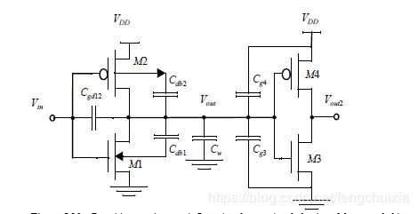
Supposed V i n V_{in} Vin has an ideal input voltage source.
-
Gate-Drain Capacitance C g d 12 C_{gd12} Cgd12
during the first half, M 1 M1 M1 is cut-off or saturation mode. The channel capacitance does not play a role here. If cut-off, it is between gate and bulk, if saturation, it is between gate and source. The capacitance is mainly the overlap capacitance.
Miller effect the capacitance-to-ground must have a value that is twice as large as the floating capacitance.
C g d = 2 C G D 0 W C_{gd} = 2C_{GD0}W Cgd=2CGD0W C G D 0 C_{GD0} CGD0 is the overlap capacitance per unit width
-
Diffusion Capacitance C d b 1 C_{db1} Cdb1 and C d b 2 C_{db2} Cdb2
the capacitance between drain and bulk.
-
Wiring Capacitance C w C_w Cw
connecting wires
-
Gate Capacitance C g 3 C_{g3} Cg3 and C g 4 C_{g4} Cg4
fanout capacitance C f a n o u t = C g a t e ( N M O S ) + C g a t e ( P M O S ) = C_{fanout} = C_{gate}(NMOS) + C_{gate}(PMOS)= Cfanout=Cgate(NMOS)+Cgate(PMOS)=
( C G S O n + C G D O n + W n L n C o x ) + ( C G S O p + C G D O p + W p L p C o x ) (C_{GSOn}+C_{GDOn}+W_nL_nC_{ox})+(C_{GSOp}+C_{GDOp}+W_pL_pC_{ox}) (CGSOn+CGDOn+WnLnCox)+(CGSOp+CGDOp+WpLpCox)
The total channel capacitance is not constant actually. varies from 2 / 3 W L C o x 2/3WLC_{ox} 2/3WLCox to the full W L C o x WLC_{ox} WLCox.
Propagation Delay :
t p = ∫ v 1 v 2 C L ( x ) i ( v ) d v t_p = \displaystyle \int^{v_2}_{v_1}{\frac{C_L(x)}{i(v)}dv} tp=∫v1v2i(v)CL(x)dv
R e q = 3 4 V D D I D S A T ( 1 − 7 9 λ V D D ) R_{eq} = {\frac{3}{4}}{\frac{V_{DD}}{I_{DSAT}}}(1-{\frac{7}{9}}\lambda V_{DD}) Req=43IDSATVDD(1−97λVDD) R e q R_{eq} Req is the average on-resistance of the MOS transistor.
t p H L = I n ( 2 ) R e q n C L = 0.69 R e q n C L t_{pHL}=In(2)R_{eqn}C_{L}=0.69R_{eqn}C_{L} tpHL=In(2)ReqnCL=0.69ReqnCL
t p L H = 0.69 R e q p C L t_{pLH} = 0.69R_{eqp}C_L tpLH=0.69ReqpCL
t p = ( t p H L + t p L H ) / 2 = 0.69 C L ( R e q n + R e q p ) / 2 t_p = (t_{pHL}+t_{pLH})/2=0.69C_L(R_{eqn}+R_{eqp})/2 tp=(tpHL+tpLH)/2=0.69CL(Reqn+Reqp)/2
R e q n R_{eqn} Reqn and R e q p R_{eqp} Reqp is the normalized on-resistances. ( W L ) (\frac{W}{L}) (LW) is ratio. the realistic resistance is R e q n / ( W / L ) R_{eqn}/(W/L) Reqn/(W/L).
If we want R e q n = = R e q p R_{eqn}==R_{eqp} Reqn==Reqp , then PMOS is wider than NMOS. However, t p H L = t p L H t_{pHL}=t_{pLH} tpHL=tpLH does not mean t p t_p tp is smallest. We can make PMOS smaller than computation
Another computation: ignore the factor λ \lambda λ
t p H L = 3 4 V D D I D S A T n ≈ 0.52 C L ( W / L ) n ( k n ) ’ V D S A T n t_{pHL}={\frac{3}{4}}{\frac{V_{DD}}{I_{DSATn}}}\approx0.52\frac{C_L}{(W/L)_n(k_n)^{’}V_{DSATn}} tpHL=43IDSATnVDD≈0.52(W/L)n(kn)’VDSATnCL
If V D D V_{DD} VDD decreases, t p H L t_{pHL} tpHL will increases.
Conclusion:
-
Reduce C L C_L CL
-
Increase the (W/L) ratio
-
Increase V D D V_{DD} VDD
7)Design for Performance
Supposed symmetrical inverter:
C L = C i n t + C e x t C_L=C_{int}+C_{ext} CL=Cint+Cext
t p = 0.69 R e q ( C i n t + C e x t ) = 0.69 R e q C i n t ( 1 + C e x t / C i n t ) = t p 0 ( 1 + C e x t / C i n t ) t_p=0.69R_{eq}(C_{int}+C_{ext})=0.69R_{eq}C_{int}(1+C_{ext}/C_{int})=t_{p0}(1+C_{ext}/C_{int}) tp=0.69Req(Cint+Cext)=0.69ReqCint(1+Cext/Cint)=tp0(1+Cext/Cint)
t p 0 t_{p0} tp0 is unloaded delay
C i n t = S C i r e f C_{int}=SC_{iref} Cint=SCiref R e q = R r e f / S R_{eq}=R_{ref}/S Req=Rref/S S S S is the sizing factor. C i r e f C_{iref} Ciref is a minimize-sized inverter.
t p = 0.69 R i r e f C i r e f ( 1 + C e x t S C i r e f ) = t p 0 ( 1 + C e x t S C i r e f ) t_p = 0.69R_{iref}C_{iref}(1+\frac{C_{ext}}{SC_{iref}})=t_{p0}(1+\frac{C_{ext}}{SC_{iref}}) tp=0.69RirefCiref(1+SCirefCext)=tp0(1+SCirefCext)
Conclusion:
if S S S is larger, t p t_p tp is smaller.
- A Chain of Inverter
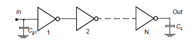
C i n t = γ C g C_{int}=\gamma C_{g} Cint=γCg γ \gamma γ is a proportionality factor. close to 1.
t p = t p 0 ( 1 + C e x t r C g ) = t p 0 ( 1 + f / γ ) t_p=t_{p0}(1+\frac{C_{ext}}{rC_g})=t_{p0}(1+f/\gamma) tp=tp0(1+rCgCext)=tp0(1+f/γ) f f f is effective fanout.
t p , j = t p 0 ( 1 + C g , j + 1 γ C g , j ) = t p 0 ( 1 + f j γ ) t_{p,j}=t_{p0}(1+\frac{C_{g,j+1}}{\gamma C_{g,j}})=t_{p0}(1+\frac{f_j}{\gamma}) tp,j=tp0(1+γCg,jCg,j+1)=tp0(1+γfj)
t p = ∑ j = 0 N t p , j = t p 0 ∑ j = 0 N ( 1 + C g , j + 1 γ C g , j ) t_p=\displaystyle \sum^{N}_{j=0}t_{p,j}=t_{p0}\displaystyle \sum^{N}_{j=0}(1+\frac{C_{g,j+1}}{\gamma C_{g,j}}) tp=j=0∑Ntp,j=tp0j=0∑N(1+γCg,jCg,j+1) C g , N + 1 = C L C_{g,N+1}=C_L Cg,N+1=CL
To make t p t_p tp min, we need each inverter is sized up by the same factor f f f.
f = C L / C g , 1 N = F N f=\sqrt[N]{C_L/C_{g,1}}=\sqrt[N]{F} f=NCL/Cg,1=NF t p = N t p 0 ( 1 + F N / γ ) t_p=Nt_{p0}(1+\sqrt[N]{F}/\gamma) tp=Ntp0(1+NF/γ)
The optimized f f f:
if γ \gamma γ equals 1, f f f is chose to be 3.6.If f f f is too small, which means N N N is too large, then t p t_p tp will be larger.
If the input signal changes gradually, PMOS and NMOS conduct simultaneously.
t s t_s ts- t p t_p tp: t p t_p tp increases linearly with t s t_s ts
So we can change t p t_p tp : t p i = t s t e p i + η t s t e p i − 1 {t_p}^{i}={t_{step}}^{i}+\eta {t_{step}}^{i-1} tpi=tstepi+ηtstepi−1
- Dynamic Power Consumption:
E V D D = C L V D D 2 E_{VDD}=C_L{V_{DD}}^{2} EVDD=CLVDD2
E o u t = C L V D D 2 2 E_{out}=\frac{C_L{V_{DD}}^{2}}{2} Eout=2CLVDD2
Half energy has been dissipated by PMOS
Conclusion: E d i s s i p a t e d = C L V D D 2 E_{dissipated} = C_L{V_{DD}}^{2} Edissipated=CLVDD2
P d y n = C L V D D 2 f 0 − > 1 P_{dyn} = C_L{V_{DD}}^{2}f_{0->1} Pdyn=CLVDD2f0−>1 f 0 − > 1 = 2 t p f_{0->1} = 2t_p f0−>1=2tp means a switched time.(on and off)
However:
switching factor f 0 − > 1 f_{0->1} f0−>1 P d y n = C L V D D 2 P 0 − > 1 f = C E F F V D D 2 f P_{dyn}=C_L{V_{DD}}^{2}P_{0->1}f=C_{EFF}{V_{DD}}^{2}f Pdyn=CLVDD2P0−>1f=CEFFVDD2f f f f is clock time
C E F F C_{EFF} CEFF effective capacitance
Solution: How to reduce power
- Reducing V D D V_{DD} VDD But V D D V_{DD} VDD need to be larger than 2 V T V_{T} VT, or the performance is bad.
- Reducing the effective capacitance
Analysis:

t p = t p 0 ( ( 1 + f / γ ) + ( 1 + F / f γ ) ) t_p=t_{p0}((1+f/\gamma)+(1+F/f\gamma)) tp=tp0((1+f/γ)+(1+F/fγ))
t p 0 t_{p0} tp0~ V D D V D D − V T E \frac{V_{DD}}{V_{DD}-V_{TE}} VDD−VTEVDD
V T E = V t + V D S A T n / 2 V_{TE} = V_{t}+V_{DSATn}/2 VTE=Vt+VDSATn/2
Conclusion: Energy & Performance
if F F F is larger, the optimal sizing factor for energy is smaller than the one for performance.
- Direct-Path Currents

E d p = V D D I p e a k t s c 2 + V D D I p e a k t s c 2 = t s c V D D I p e a k E_{dp}=V_{DD}\frac{I_{peak}t_{sc}}{2}+V_{DD}\frac{I_{peak}t_{sc}}{2}=t_{sc}V_{DD}I_{peak} Edp=VDD2Ipeaktsc+VDD2Ipeaktsc=tscVDDIpeak
P d p = t s c V D D I p e a k f = C s c V D D 2 f P_{dp}=t_{sc}V_{DD}I_{peak}f=C_{sc}{V_{DD}}^{2}f Pdp=tscVDDIpeakf=CscVDD2f
t s c = V D D − 2 V T V D D t s t_{sc}=\frac{V_{DD}-2V_{T}}{V_{DD}}t_{s} tsc=VDDVDD−2VTts
t s c t_{sc} tsc represents the time both devices are conducting.
t s t_s ts represents the 0-100% transition time.
If we want to decrease the direct-path dissipation, we need to make t p t_p tp larger.
- Static consumption
P s t a t = I s t a t V D D P_{stat} = I_{stat}V_{DD} Pstat=IstatVDD I s t a t I_{stat} Istat is a leakage current
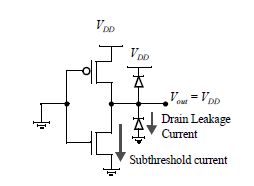
- subtheshold current solution: SOI
- drain leakage current
- Put it all together
P t o t = P d y n + P d p + P s t a t P_{tot} = P_{dyn}+P_{dp}+P_{stat} Ptot=Pdyn+Pdp+Pstat
PDP power-delay product: P D P = P a v t p PDP=P_{av}t_p PDP=Pavtp average energy consumed per switching event
P D P = C L V D D 2 f m a x t p = C L V D D 2 2 PDP = C_L{V_{DD}}^{2}f_{max}t_{p}=\frac{C_L{V_{DD}}^{2}}{2} PDP=CLVDD2fmaxtp=2CLVDD2
switching event means 0->1 or 1->0 transition
E a v E_{av} Eav is twice the PDP
EDP energy-delay product: combine a measure of performance and energy
E D P = C L V D D 2 2 t p EDP = \frac{C_L{V_{DD}}^{2}}{2}t_p EDP=2CLVDD2tp
High supply voltage reduce delay, but harm the energy
Conclusion:
V D D o p t = 3 2 V T E V_{DDopt}=\frac {3}{2} V_{TE} VDDopt=23VTE
- Scaling technology
The interconnect component