【FPGA】Buffer专题介绍(一)
目录
背景
BUFG
BUFGCE
BUFGCE_1
BUFGMUX and BUFGMUX_1
BUFGP
BUFH
BUFIO2
BUFIO2FB
背景
在数据手册 Spartan-6 Libraries Guide for HDL Designs中看到了有关buffer的一些介绍,这里就根据掌握简记之。
从手册的开头声明,或许可以看出看这些东西有什么用途:
This HDL guide is part of the ISE documentation collection. A separate version of this guide is available if you prefer to work with schematics.
This guide contains the following:
• Introduction.
• A list of design elements supported in this architecture, organized by functional categories.
• Individual descriptions of each available primitive.
此HDL指南是ISE文档集的一部分。 如果您更喜欢使用原理图,可以使用本指南的单独版本。
本指南包含以下内容:
• 介绍。
•此体系结构中支持的设计元素列表,按功能类别组织。
•每个可用原语的单独描述。
即便如此,即使我不喜欢用原理图设计,了解这部分知识也大有裨益,作为一个硬件工作中,怎么能不了解FPGA设计中支持的设计元素呢?并且一些原语的描述对于我们了解它们在FPGA电路中的作用是很有帮助的。
在正式介绍本部分知识之前,还有必要掌握一些前提性的知识:
For each design element in this guide, Xilinx evaluates the four options and recommends what we believe is the best solution for you. The four options are:
• Instantiation - This component can be instantiated directly into the design. This method is useful if you want to control the exact placement of the individual blocks.
• Inference - This component can be inferred by most supported synthesis tools. You should use this method if you want to have complete flexibility and portability of the code to multiple architectures. Inference also gives the tools the ability to optimize for performance, area, or power, as specified by the user to the synthesis tool.
• Coregen & Wizards - This component can be used through Coregen or Wizards. You should use this method if you want to build large blocks of any FPGA primitive that cannot be inferred. When using this flow, you will have to re-generate your cores for each architecture that you are targeting.
• Macro Support - This component has a UniMacro that can be used. These components are in the UniMacro library in the Xilinx tool, and are used to instantiate primitives that are complex to instantiate by just using the primitives. The synthesis tools will automatically expand the unimacros to their underlying primitives.
对于本指南中的每个设计元素,Xilinx评估了四个选项,并推荐我们认为最适合您的解决方案。 四个选项是:
•实例化 - 可以将此组件直接实例化到设计中。 如果要控制各个块的确切位置,此方法很有用。
buffer原语一般只需要实例化就可以用了。
•推理 - 大多数支持的综合工具都可以推断出该组件。 如果希望将代码具有完全的灵活性和可移植性,则应使用此方法。 推理还使工具能够根据用户对综合工具的指定来优化性能,面积或功率。
这个我还不是太了解,我们还是用到了再分析吧。
•Coregen和Wizards - 此组件可通过Coregen或Wizards使用。 如果要构建无法推断的任何FPGA原语的大块,则应使用此方法。 使用此方法时,您必须为要定位的每个体系结构重新生成核。
这个就比较常见了,就是产生一个IP核。
•宏支持 - 该组件具有可以使用的UniMacro。 这些组件位于Xilinx工具的UniMacro库中,用于实例化一些很难仅通过原语实例化的原语。 综合工具将自动将unimacros扩展到其底层原语。
宏就是赛灵思提供的一些硬件宏,例如MUX,RAM等。
好了,大致了解这么多就可以了,本博文是有关buffer的专题介绍,那就开始这块内容了。
BUFG
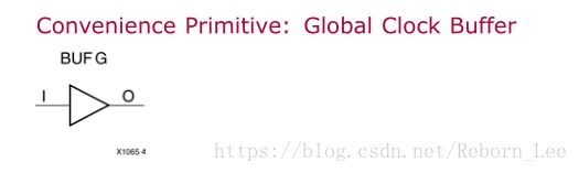
全局时钟Buffer
This design element is a high-fanout buffer that connects signals to the global routing resources for low skew distribution of the signal. BUFGs are typically used on clock nets.
该设计元素是一个高扇出缓冲器,它将信号连接到全局布线资源,以实现信号的低偏斜分布。 BUFG通常用于时钟网。

可以使用实例化(Instantiation),Verilog HDL的实例化模板如下:
Verilog Instantiation Template
// BUFG: Global Clock Buffer (source by an internal signal)
// All FPGAs
// Xilinx HDL Libraries Guide, version 11.2
BUFG BUFG_inst (
.O(O), // Clock buffer output
.I(I) // Clock buffer input
);
// End of BUFG_inst instantiation
BUFGCE

带有时钟使能的全局时钟Buffer
This design element is a global clock buffer with a single gated input. Its O output is "0" when clock enable (CE) is Low (inactive). When clock enable (CE) is High, the I input is transferred to the O output.
此设计元素是具有单门控输入的全局时钟缓冲器。 当时钟使能(CE)为低(无效)时,其O输出为“0”。 当时钟使能(CE)为高电平时,I输入被传送到O输出。

Verilog 例化模板如下:
Verilog Instantiation Template
// BUFGCE: Global Clock Buffer with Clock Enable (active high)
// Virtex-4/5/6, Spartan-3/3E/3A/6
// Xilinx HDL Libraries Guide, version 11.2
BUFGCE BUFGCE_inst (
.O(O), // Clock buffer output
.CE(CE), // Clock enable input
.I(I) // Clock buffer input
);
// End of BUFGCE_inst instantiation
BUFGCE_1
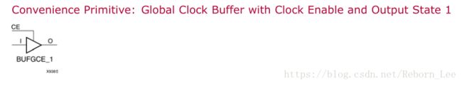
与BUFGCE的区别在于时钟使能(CE)为0时,输出状态为1。
This design element is a multiplexed global clock buffer with a single gated input. Its O output is High (1) when clock enable (CE) is Low (inactive). When clock enable (CE) is High, the I input is transferred to the O output.
该设计元素是具有单门控输入的多路复用全局时钟缓冲器。 当时钟使能(CE)为低(无效)时,其O输出为高(1)。 当时钟使能(CE)为高电平时,I输入被传送到O输出。

Verilog HDL例化模板:
Verilog Instantiation Template
// BUFGCE_1: Global Clock Buffer with Clock Enable (active low)
// Virtex-4/5/6, Spartan-3/3E/3A/6
// Xilinx HDL Libraries Guide, version 11.2
BUFGCE_1 BUFGCE_1_inst (
.O(O), // Clock buffer output
.CE(CE), // Clock enable input
.I(I) // Clock buffer input
);
// End of BUFGCE_1_inst instantiation
BUFGMUX and BUFGMUX_1


BUFGMUX is a multiplexed global clock buffer that can select between two input clocks: I0 and I1. When the select input (S) is Low, the signal on I0 is selected for output (O). When the select input (S) is High, the signal on I1 is selected for output.
BUFGMUX and BUFGMUX_1 are distinguished by the state the output assumes when that output switches between clocks in response to a change in its select input. BUGFMUX assumes output state 0 and BUFGMUX_1 assumes output state 1.
BUFGMUX是一个多路复用的全局时钟缓冲器,可以在两个输入时钟之间进行选择:I0和I1。 当选择输入(S)为低时,选择I0上的信号作为输出(O)。 当选择输入(S)为高电平时,选择I1上的信号进行输出。
BUFGMUX和BUFGMUX_1的区别在于当输出在时钟之间切换以响应其选择输入的变化时输出的状态。 BUGFMUX假定输出状态为0,BUFGMUX_1为输出状态1。
Note: BUFGMUX guarantees that when S is toggled, the state of the output remains in the inactive state until the next active clock edge (either I0 or I1) occurs.
注意:BUFGMUX保证当S切换时,输出状态保持无效状态,直到出现下一个有效时钟沿(I0或I1)。

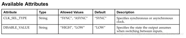
这个Available Attributes是什么意思呢?
字面上翻译是可用的属性:
CLK_SEL_TYPE:Specifies synchronous or asynchronous clock.
指定同步或异步时钟。默认为同步时钟(SYNC)。
DISABLE_VALUE:Specifies the state the output assumes when switching between inputs.
指定输入之间切换时输出的状态。默认的是低电平(LOW)。
Verilog 例化模板:
Verilog Instantiation Template
// BUFGMUX: Global Clock Buffer 2-to-1 MUX
// Spartan-3/3E/3A/6
// Xilinx HDL Libraries Guide, version 11.2
BUFGMUX BUFGMUX_inst (
.O(O), // Clock MUX output
.I0(I0), // Clock0 input
.I1(I1), // Clock1 input
.S(S) // Clock select input
);
// End of BUFGMUX_inst instantiation
下面贴出BUFGMUX_1的真值表,BUFGMUX_1与BUFGMUX的区别仅仅是选择输入变化时,输出的状态,BUFGMUX_1输出的状态为1,BUFGMUX输出的状态为0,如下图:
 、
、
下面给出实例模板:
Verilog Instantiation Template
// BUFGMUX_1: Global Clock Buffer 2-to-1 MUX (inverted select)
// Spartan-3/3E/3A/6
// Xilinx HDL Libraries Guide, version 11.2
BUFGMUX_1 BUFGMUX_1_inst (
.O(O), // Clock MUX output
.I0(I0), // Clock0 input
.I1(I1), // Clock1 input
.S(S) // Clock select input
);
// End of BUFGMUX_1_inst instantiation
BUFGP

用于驱动时钟或延长线的主要全局缓冲器
This design element is a primary global buffer that is used to distribute high fan-out clock or control signals throughout in FPGA devices. It is equivalent to an IBUFG driving a BUFG.
This design element provides direct access to Configurable Logic Block (CLB) and Input Output Block (IOB) clock pins and limited access to other CLB inputs. The input to a BUFGP comes only from a dedicated IOB.
Because of its structure, this element can always access a clock pin directly. However, it can access only one of the F3, G1, C3, or C1 pins, depending on the corner in which the BUFGP is placed. When the required pin cannot be accessed directly from the vertical line, PAR feeds the signal through another CLB and uses general purpose routing to access the load pin.
该设计元素是主要的全局缓冲区,用于在FPGA器件中分配高扇出时钟或控制信号。 它相当于驾驶BUFG的IBUFG。
该设计元素提供对可配置逻辑块(CLB)和输入输出块(IOB)时钟引脚的直接访问以及对其他CLB输入的有限访问。 BUFGP的输入仅来自专用IOB。
由于其结构,该元件可以始终直接访问时钟引脚。 但是,它只能访问F3,G1,C3或C1引脚中的一个,具体取决于放置BUFGP的角落。 当无法直接从垂直线访问所需的引脚时,PAR通过另一个CLB馈送信号,并使用通用布线(routing)访问负载引脚。

BUFH

单个时钟区域的时钟缓冲器
The BUFH primitive is provided to allow instantiation capability to access the HCLK clock buffer resources.
提供BUFH原语以允许实例化能力访问HCLK时钟缓冲器资源。

Verilog Instantiation Template
// BUFH: Clock buffer for a single clocking region
// Virtex-6
// Xilinx HDL Language Template, version 11.4
BUFH BUFH_inst (
.O(O), // 1-bit The output to the BUFH
.I(I) // 1-bit The input to the BUFH
);
// End of BUFH_inst instantiation
BUFIO2

双时钟缓冲器和选通脉冲
This primitive takes a clock input and generates two clock outputs and a strobe pulse. The IOCLK output is a buffered version of the input clock. The period and duty cycle of the DIVCLK output is dependent on the attribute setting. If the DIVIDE_BYPASS is set to TRUE then the DIVCLK output is a buffered version of the input clock and the SERDESSTOBE output is driven to 1. If DIVIDE_BYPASS is set to FALSE then the DIVCLK and SERDESSTROBE output are divided input clock by the setting of the divide attribute.
该原语采用时钟输入并产生两个时钟输出和一个选通脉冲。 IOCLK输出是输入时钟的缓冲版本。 DIVCLK输出的周期和占空比取决于属性设置。 如果DIVIDE_BYPASS设置为TRUE,则DIVCLK输出是输入时钟的缓冲版本,SERDESSTOBE输出驱动为1.如果DIVIDE_BYPASS设置为FALSE,则DIVCLK和SERDESSTROBE输出通过除法设置分频输入时钟 属性。

Verilog Instantiation Template
// BUFIO2: Dual Clock Buffer and Strobe Pulse
// Spartan-6
// Xilinx HDL Language Template, version 11.1
BUFIO2 #(
.DIVIDE(1), // Set the DIVCLK divider divide-by value.
.DIVIDE_BYPASS("TRUE"), // DIVCLK output sourced from Divider (FALSE) or from I input, bypassing Divider
// (TRUE).
.I_INVERT("FALSE"),
.USE_DOUBLER("FALSE")
)
BUFIO2_inst (
.DIVCLK(DIVCLK), // 1-bit Output divided clock
.IOCLK(IOCLK), // 1-bit Output clock
.SERDESSTROBE(SERDESSTROBE), // 1-bit Output SERDES strobe (Clock Enable)
.I(I) // 1-bit Clock input
);
// End of BUFIO2_inst instantiation
BUFIO2FB

This component is a simple buffer that has an attribute to determine the output delay. If DIVIDE_BYPASS is set to TRUE then the delays are equivalent to the BUFIO2 bypass delay. When set to FALSE, the delays are similar to the BUFIO2 DIVCLK outputs to keep the outputs of the BUFIO2 and BUFIO2FB phase aligned.
该组件是一个简单的缓冲区,具有确定输出延迟的属性。 如果DIVIDE_BYPASS设置为TRUE,则延迟等同于BUFIO2旁路延迟。 设置为FALSE时,延迟类似于BUFIO2 DIVCLK输出,以保持BUFIO2和BUFIO2FB相位的输出对齐。

DIVIDE_BYPASS
DIVCLK output sourced from Divider (FALSE) or from I input, bypassing Divider (TRUE). If FALSE, also need to set CLKDIV DIVIDE value to 1.
DIVCLK输出来自Divider(FALSE)或I输入,绕过Divider(TRUE)。 如果为FALSE,还需要将CLKDIV DIVIDE值设置为1。
Verilog Instantiation Template
// BUFIO2FB: Feedback Clock Buffer
// Spartan-6
// Xilinx HDL Language Template, version 11.1
BUFIO2FB #(
.DIVIDE_BYPASS("TRUE") // DIVCLK output sourced from Divider (FALSE) or from I input, bypassing Divider
// (TRUE) Note: if FALSE, also need to set CLKDIV DIVIDE value to 1.
)
BUFIO2FB_inst (
.O(O), // 1-bit Output feedback clock
.I(I) // 1-bit Feedback clock input
);
// End of BUFIO2FB_inst instantiation
先记到这里,这种类似的Buffer太多了,下一篇继续总结。
【FPGA】Buffer专题介绍(二)