简单计算机系统综合设计(CPU)
简单计算机系统综合设计(CPU)
前言:作为一位来自于湖南大学的本科生,让我最难忘记的就是这一次CPU的综合设计了。学软件的我,贴一篇硬件编程没啥意思,纯当打发时间。
基本部件
数字逻辑实验中我们要求完成的有以下基本部件,使用VHDL源完成编程。
0000:指令寄存器IR,
a) 模块的接口设计
控制信号:LDIR,CLK,I[7…0]
输入信号:需执行指令I[7…0] 输出信号:需执行指令out1[7…0]
b) 功能实现
根据指令寄存器IR的功能可知:
当HALT = 1 时,输出信号 x[7…0] 为高阻态;
否则,当处于时钟下降沿时,LDIR = 1时,输出信号out[7…0]为输入信号I[7…0]。
VHDL的实现如下所示:
library ieee;
use ieee.std_logic_1164.all;
entity IR is
	port (LDIR, CLK : in std_logic;
		I : in std_logic_vector(7 downto 0);
		OUT1 : out std_logic_vector(7 downto 0)
		);
end IR;

architecture behavior of IR is
	signal command: std_logic_vector(7 downto 0);
	begin
		OUT1 <= command;
		process(CLK)
			begin
				if (CLK'event and CLK = '0' and LDIR = '1') then
					command <= I;
				end if;
			end process;
end behavior;
0001:指令译码器DECODING,
a) 模块的接口设计
控制信号:EN 输入信号:需执行指令IR[7…0]
输出信号:需执行指令IR[7…0],
各项指令的控制信号:MOVA,MOVB,MOVC,ADD,SUB,OR1,NOT1,RSR,RSL,JMP,JZ,JC,IN1,OUT1,NOP,HALT
b) 功能实现
根据指令译码器的功能可知:
当EN = 1时,输入信息:需执行指令IR[7…0]对应一个指令控制信号。
指令译码器需要完成指令机器码和指令控制信号的一一对应。
VHDL的实现如下所示:
library ieee;
use ieee.std_logic_1164.all;

entity DECODING is
port(EN:in std_logic;
	 IR:in std_logic_vector(7 downto 0);
	 MOVA, MOVB, MOVC, ADD, SUB, OR1, NOT1, RSR, RSL, JMP, JZ, JC, IN1, OUT1, NOP, HALT: out std_logic);
end DECODING;

architecture behavior of DECODING is
signal R: std_logic_vector(7 downto 0):="00000000";
signal signalB,signalC: std_logic;
begin
	MOVA <= '1' when
	IR(7 downto 4) = "1111" and (not (IR(3 downto 2) = "11")) and (not (IR(1 downto 0) = "11")) and EN = '1' else '0';
	MOVB <= '1' when
	IR(7 downto 4) = "1111" and (IR(3 downto 2) = "11") and (not (IR(1 downto 0) = "11")) and EN = '1' else '0';
	MOVC <= '1' when
	IR(7 downto 4) = "1111" and (not (IR(3 downto 2) = "11")) and (IR(1 downto 0) = "11") and EN = '1' else '0';
	ADD <= '1' when
	IR(7 downto 4) = "1001" and EN = '1' else '0';
	SUB <= '1' when
	IR(7 downto 4) = "0110" and EN = '1' else '0';
	OR1 <= '1' when
	IR(7 downto 4) = "1011" and EN = '1' else '0';
	NOT1 <= '1' when
	IR(7 downto 4) = "0101" and EN = '1' else '0';
	RSR <= '1' when
	IR(7 downto 4) = "1010" and (IR(1 downto 0) = "00") and EN = '1' else '0';
	RSL <= '1' when
	IR(7 downto 4) = "1010" and (IR(1 downto 0) = "11") and EN = '1' else '0';
	JMP <= '1' when
	IR(7 downto 0) = "00010000" and EN = '1' else '0';
	JZ <= '1' when
	IR(7 downto 0) = "00010001" and EN = '1' else '0';
	JC <= '1' when
	IR(7 downto 0) = "00010010" and EN = '1' else '0';
	IN1 <= '1' when
	IR(7 downto 4) = "0010" and EN = '1' else '0';
	OUT1 <= '1' when
	IR(7 downto 4) = "0100" and EN = '1' else '0';
	NOP <= '1' when
	IR(7 downto 0) = "01110000" and EN = '1' else '0';
	HALT <= '1' when
	IR(7 downto 0) = "10000000" and EN = '1' else '0';

end behavior;
0010:控制信号产生逻辑 LOGIC,
a) 模块的接口设计
控制信号:SM
输入信号:MOVA,MOVB,MOVC,ADD,SUB,OR1,NOT1,RSR,RSL,JMP,JZ,JC,IN1,OUT1,NOP,HALT,C,Z
输出信号:INPC,LDPC,LDIR,WE,FBUS,FLBUS,FRBUS,CS,DL,XL,M,HALT_out
b) 功能实现
当SM = 1时,输入信息:需执行指令IR[7…0]对应一个指令控制信号。
指令译码器需要完成指令机器码和指令控制信号的一一对应。
VHDL的实现如下所示:
library ieee;
use ieee.std_logic_1164.all;
entity control_logism is
       port(SM,MOVA,MOVB,MOVC,ADD,SUB,OR1,NOT1,RSR,RSL,JMP,JZ,JC,IN1,OUT1,NOP,HALT,C,Z:in std_logic;
            IR: in std_logic_vector(7 downto 0);
            RAA,RWBA,MADD: out std_logic_vector(1 downto 0);
            S: out std_logic_vector(3 downto 0);
            INPC,LDPC,LDIR,WE,FBUS,FLBUS,FRBUS,CS,DL,XL,M,HALT_out: out std_logic
            );
end control_logism;

architecture control_logism_behavior of control_logism is
begin
	process(MOVA,MOVB,MOVC,ADD,SUB,OR1,NOT1,RSR,RSL,JMP,JZ,JC,C,Z,IN1,OUT1,NOP,HALT,IR)
	  begin
		S(3) <= IR(7);
		S(2) <= IR(6);
		S(1) <= IR(5);
		S(0) <= IR(4);
		LDIR <= not SM;
		INPC <= (not SM);
		LDPC <= JMP or (Z and JZ) or (C and JC);
		WE <= ((not MOVA) and (not MOVC) and (not ADD) and (not SUB) and (not OR1) and (not NOT1) and (not RSR) and (not RSL) and (not IN1)) or (not SM);
		RAA <= IR(1 downto 0);
		RWBA <= IR(3 downto 2);
		M <= ADD or SUB or OR1 or NOT1;
		FBUS <= MOVA or MOVB or ADD or SUB or OR1 or NOT1 or OUT1;
		FLBUS <= RSL;
		FRBUS <= RSR;
		DL <= (not SM) or MOVC or JMP or JC or JZ;
		XL <= MOVB;
		MADD(1) <= MOVB;
		MADD(0) <= MOVC;
		HALT_out <= HALT;
	end process;
end control_logism_behavior;
0011:函数发生器ALU,
a) 控制信号:M,S[3…0]
输入信号:数据A[7…0],B[7…0]
输出信号:数据COUT[7…0],C,Z
b) 功能实现
根据函数发生器ALU的功能可知:
根据 M,S[3…0],需要判断:
对数据进行加法运算,减法运算,或运算,取反运算还是不处理;
根据数据A[7…0],B[7…0],可以得到各种运算的结果;
通过运算结果可以得到输出的数据COUT[7…0],以及C,Z
函数发生器ALU需要完成:
对A口,B口进入的数据进行各种运算并且处理输出结果。
VHDL的实现如下所示:
library ieee;
use ieee.std_logic_1164.all;
use ieee.std_logic_unsigned.all;
use ieee.std_logic_arith.all;
entity model_operator_ALU is

	port (
		m : in std_logic;
		s : in std_logic_vector(3 downto 0);
		a, b : in std_logic_vector(7 downto 0);
		T : out std_logic_vector(7 downto 0);
		cf, zf : out std_logic);
end model_operator_ALU;

architecture Behavior of model_operator_ALU is
	signal temp : std_logic_vector(8 downto 0);
	signal pf,pf2 : std_logic_vector(0 downto 0);
	begin
	pf <= "0";
	pf2 <= "1";
	with m&s select
		temp <= (pf&b) + (pf&a) when "11001",
			(pf2&b) - (pf&a) when "10110",
			(pf&b) or (pf&a) when "11011",
			not (pf&b) when "10101",
			pf&a when "11111",
			pf&a when "01111",
			pf&b when "11010",
			pf&b when "01010",
			pf&b when "00100",
			pf&b when "10100",
			"011111111" when others;
	T <= temp(7 downto 0);
	cf <= temp(8);
	zf <= not(temp(8) or temp(7) or temp(6) or temp(5) or temp(4) or temp(3) or temp(2) or temp(1) or temp(0));
end Behavior;
0100:移位逻辑SHIFT,
a) 控制信号:FBUS,FLBUS,FRBUS
输入信号:数据a[7…0] 输出信号:数据 w[7…0],cf
b) 功能实现
根据移位逻辑的功能可知:
当FBUS = 1时,输出数据 w[7…0]为输入数据a[7…0];
当FLBUS = 1时,输出数据 w[7…0]为输入数据a[7…0]的逻辑左移;
当FRBUS = 1时,输出数据 w[7…0]为输入数据a[7…0]的逻辑右移;
通过结果可以得到cf;
移位逻辑需要完成:对输入数据a[7…0]进行逻辑移位并且处理输出结果。
VHDL的实现如下所示:
library ieee;
use ieee.std_logic_1164.all;

entity shift_logic is
   port(fbus,flbus,frbus: in std_logic;
        a: in std_logic_vector(7 downto 0);
        cf: out std_logic;
        w: out std_logic_vector(7 downto 0));
end shift_logic;

architecture behavior of shift_logic is
begin
  process(fbus,flbus,frbus)
    begin
     if (flbus = '1' ) then
     w <= a(6 downto 0) & '0';
     cf <= a(7);
     elsif (frbus = '1' ) then
     w <= '0' & a(7 downto 1) ;
     cf <= a(0);
     elsif (fbus = '1') then
     w <= a;
     elsif (fbus = '0') then
     w <= "ZZZZZZZZ";
     end if;
  end process;
end behavior;
0101:使能信号SM,
a) 控制信号:CLK,EN 输出信号:SM
b) 功能实现
根据SM信号发生器的功能可知:
当处于时钟下降沿时,输出信号与之前状态的输出信号相反。
VHDL的实现如下所示:
library ieee;
use ieee.std_logic_1164.all;
use ieee.std_logic_unsigned.all;
use ieee.numeric_std.all;
entity SM_fun is
   port (CLK,EN: in std_logic;
   SM: out std_logic);
end SM_fun;
architecture behavior of SM_fun is
signal ls: std_logic:='0';
begin
  process(CLK,EN)
    begin
       if (CLK'event and (CLK = '0') and (EN = '1')) then
           ls <= not ls;
       end if;
  end process;
  SM <= ls;
end behavior;
0110:指令计数器PC,
a) 模块的接口设计
控制信号:LDPC,INPC,clk
输入数据:地址值 indata[7…0] 输出数据:地址值 outdata[7…0]
b) 功能实现
根据指令计数器PC的功能可知:
在时钟的下降沿,若LDPC = 1,输入外部的地址值,并输出该地址值;
若INPC = 1,将原先的地址值加一,并输出该地址值。
VHDL实现如下所示:
library ieee;
use ieee.std_logic_1164.all;
use ieee.std_logic_arith.all;
use ieee.std_logic_unsigned.all;
entity Instruction_counter_PC is
   port(LDPC,INPC,CLK: in std_logic;
   indata: in std_logic_vector(7 downto 0);
   outdata: out std_logic_vector(7 downto 0));
end Instruction_counter_PC;

architecture behavior of Instruction_counter_PC is
signal pc: std_logic_vector(7 downto 0):= "00000000";
begin
  process(LDPC,INPC,CLK)
    begin
      if (CLK'EVENT and CLK = '0' and INPC = '1' and LDPC = '0') then
        pc <= pc + 1;
          elsif (CLK'EVENT and CLK = '0' and INPC = '0' and LDPC = '1') then
            pc <= indata;
      end if;
      outdata <= pc;
  end process;
end behavior;
0111:通用寄存器组REGISTER,
a) 模块的接口设计
控制信号:WE,RAA[1…0],RWBA[1…0],clk
输入信号:总线数据I[7…0]
输出信号:AO[7…0],BO[7…0]
CHECK: register_A [7…0],register_B[7…0],register_C [7…0]
b) 功能实现
根据通用寄存器组的功能可知:
当处于时钟下降沿时,当WE = 0时:
根据 RWBA[1…0],需要向通用寄存器组中存入数据;
根据 RAA[1…0],RWBA[1…0],向A口和B口输出数据
通用寄存器组需要完成:
对寄存器A,寄存器B,寄存器C进行数据的输入和输出。
VHDL的实现如下所示:
library ieee;
use ieee.std_logic_1164.all;

entity Universal_register_group is
port(
	RA : in std_logic_vector(1 downto 0);
	WA : in std_logic_vector(1 downto 0);
	I : in std_logic_vector(7 downto 0);
	WE : in std_logic;
	clk : in std_logic;
	AO : out std_logic_vector(7 downto 0);
	BO : out std_logic_vector(7 downto 0);
	register_A : out std_logic_vector(7 downto 0);
	register_B : out std_logic_vector(7 downto 0);
	register_C : out std_logic_vector(7 downto 0));
end Universal_register_group;

architecture behavior of Universal_register_group is
	signal A : std_logic_vector(7 downto 0) := "00000011";
	signal B : std_logic_vector(7 downto 0) := "00001100";
	signal C : std_logic_vector(7 downto 0) := "00110000";
	begin
--Output operation
  process(clk)
	begin
		if(clk'event and clk = '0')then
			if(WE = '0') then
				if(WA = "00")then
					A <= I;
				elsif(WA = "01")then
					B <= I;
				elsif(WA = "10")then
					C <= I;
				end if;
			end if;
		end if;
  end process;
--output operation
  AO <= A when RA = "00" else
		B when RA = "01" else
		C when RA = "10" or RA = "11";
  BO <= A when WA = "00" else
		B when WA = "01" else
		C when WA = "10" or WA = "11";
  register_A <= A;
  register_B <= B;
  register_C <= C;
end behavior;
1000:选择器SELECTOR
a) 模块的接口设计
控制信号:MADD
输入信号:I0[7…0],I1[7…0],I2[7…0] 输出信号:OUT1[7…0]
b) 功能实现
根据选择器的功能可知:
当MADD = 00时,输出信息 COUT[7…0] 输入信息 S0[7…0];
当MADD = 01时,输出信息 COUT[7…0] 输入信息 S1[7…0];
当MADD = 10时,输出信息 COUT[7…0] 输入信息 S2[7…0]。
VHDL的实现如下所示:
library ieee;
use ieee.std_logic_1164.all;

entity selector is
	port (MADD : in std_logic_vector(1 downto 0);
		I0, I1, I2 : in std_logic_vector(7 downto 0);
		OUT1 : out std_logic_vector(7 downto 0)
		);
end selector;

architecture behavior of selector is
begin
	OUT1 <= I0 when MADD = "00"
		else I1 when MADD = "01"
		else I2 when MADD = "10"
		else "ZZZZZZZZ" when MADD = "11";
end behavior;
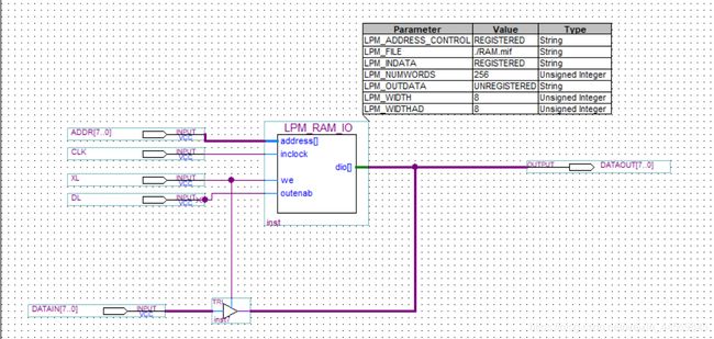
1001:存储器RAM,
a) 模块的接口设计
控制信号:inclock ( clk ),we (XL),outenab(DL)
输入信号:address[7…0] 输出信号:dio[7…0]
b) 功能实现
CPU逻辑图
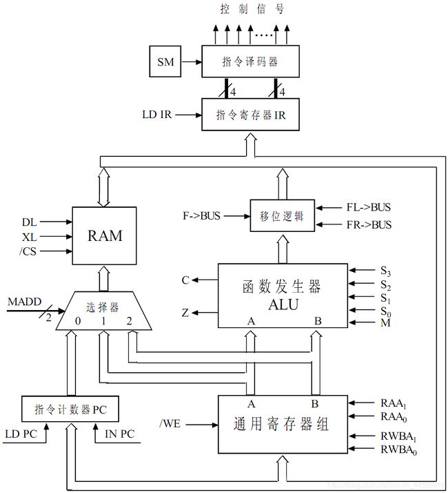
CPU逻辑图

总结
模型机的设计坑比较多
下面我分类记录了一下:
1:process的应用:我在仿真时发现信号输出的值一直是预定义信号,后来发现是因为process只能够响应信号的变化,在信号一直为某一个值时,process不会作出响应。因此,除了带有时钟信号的部件,我一律弃用了process,改为并行。
2.无论我执行哪一个指令,发现通用寄存器组的输出一直为0,因此我额外增加了register_A, register_B, register_C来CHECK我的信号,最后发现使我的BUS总线没有输入,因此我追溯到了我的ALU部分,原来是这里阻塞了信号,使得ALU和shift_logic的输出一直为高阻态,导致BUS总线一直是高阻态。
3.我的指令译码器在开始时也是没有输出的,在此之前我曾将重写了指令译码器,发现是因为指令译码器内部输入和信号搞反了,这也算是一个低级错误了吧。
4.在设计CPU的时候,连线是一个较大的问题,因为好多的信号都会串在一起,因此可以采用不直接连线,而是通过端口的名称定义为相同,从而间接将它们连接起来。
注:
本篇博客仅用作学习交流使用,新学者还是建议还是自己敲一遍。