Xilinx 7Series Clocking Architecture——个人整理
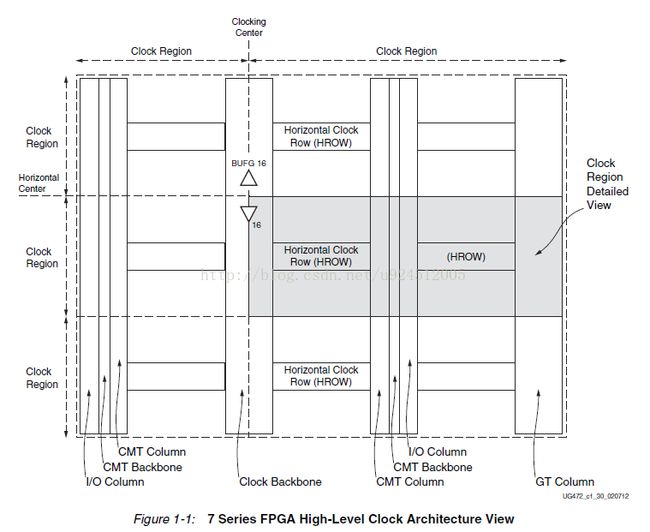
1. The vertical clocking center line (the clock backbone) divides the device into adjacent left and right regions while the horizontal center line divides the device into its top and bottom sides.
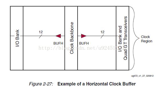
2. The horizontal clock buffers (BUFH) drive through the HROW to every clocking point in the region. BUFGs and BUFHs share routing tracks in the HROW. The I/O buffers (BUFIO) and regional clock buffers (BUFR) are located inside the I/O banks. The BUFIO only drives I/O clocking resources while the BUFR drives I/O resources and logic resources. The BUFMR enables multi-region chaining of BUFIOs and BUFRs.
BUFG and BUFH share 12 routing tracks in the HROW and can drive all clocking points in the region. BUFGs can also drive BUFHs (not shown in Figure 1-4). This allows for individual clock enables (CE) on an otherwise global clock distribution. A GT quad has ten dedicated tracks to drive the CMT and clock buffers in the clock backbone. The BUFRs located in the I/O bank have four tracks driving clocking points in the logic, CMT, and BUFG. CMTs can, with limitations, drive other CMTs in the adjacent regions using the CMT backbone. Similarly, clock-capable pins can drive, with the same limitations, CMTs in adjacent regions. Clock-capable pins can drive BUFGs anywhere in the same top/bottom side of the device. There are four tracks in the CMT backbone to support connectivity between vertical regions.
Clock sources from one region can drive clock buffer resources in its own region as well as in a horizontally adjacent region. CMTs, clock-capable pins, and serial transceivers can drive clocks into the horizontal adjacent region via the BUFH and also connect to the BUFGs in the same top/bottom side of the device.
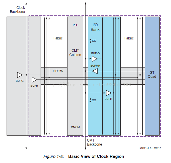
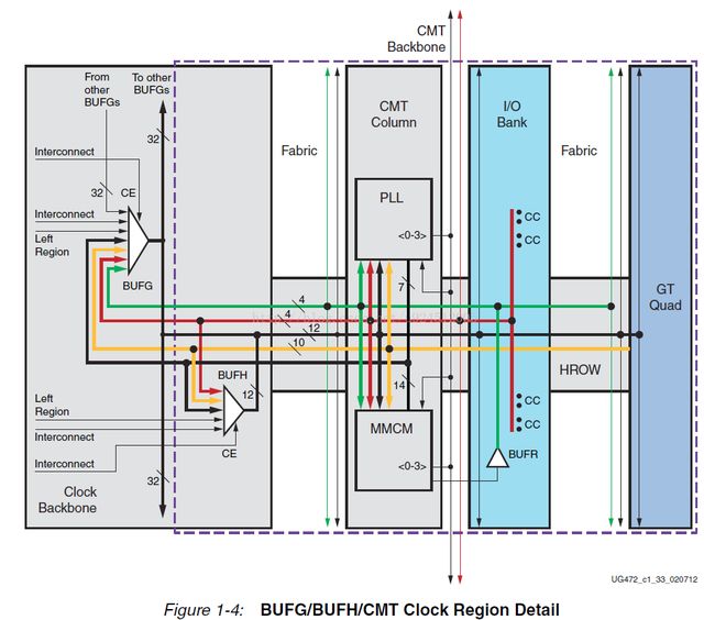
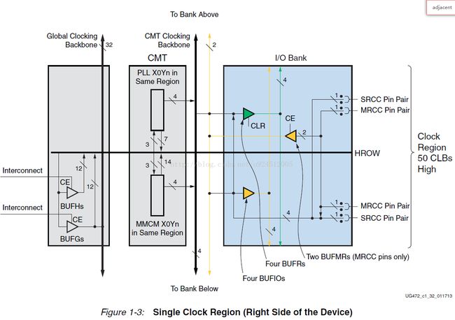
Each I/O bank contains four BUFIOs and four BUFRs. Each of these clock buffers can be driven by a specific clock-capable input clock pin pair or can be driven directly by a specific output clock of the MMCM. Two of the clock-capable input pin pairs, called MRCCs, support a multi-region clocking scheme. An MRCC pin pair can drive a specific BUFMR, which in turn can drive BUFIOs and BUFRs in the same and adjacent regions facilitating multi-region/bank interfaces. Similarly, a GT quad can also drive the BUFMRs.
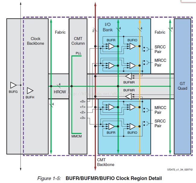
3. The main purpose of the BUFR and BUFIO combination is to support source-synchronous interfaces. When an interface is placed into a single region, the BUFIO clocks the high-speed side of the SelectIOs and the BUFR clocks the deserialized/serialized side at a lower speed into the FPGA logic providing the clock domain transfer function
4. The horizontal clock buffer BUFH (BUFHCE) is strictly a regional resource and cannot span clock regions above or below. Unlike BUFR, BUFH does not have the ability to divide the clock.
5. BUFHs are the preferred clocking resource when an interface or cloud of logic can be localized to one clock region or two horizontally adjacent clock regions.
6. BUFG、BUFH、BUFIO、BUFR
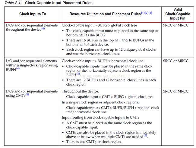
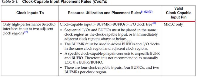
7. Single-ended clock inputs must be assigned to the P (master) side of the clock-capable input pin pair.If a single-ended clock is connected to the P-side of a differential clock pin pair, the N-side cannot be used as another single-ended clock pin—it can only be used as a user I/O.
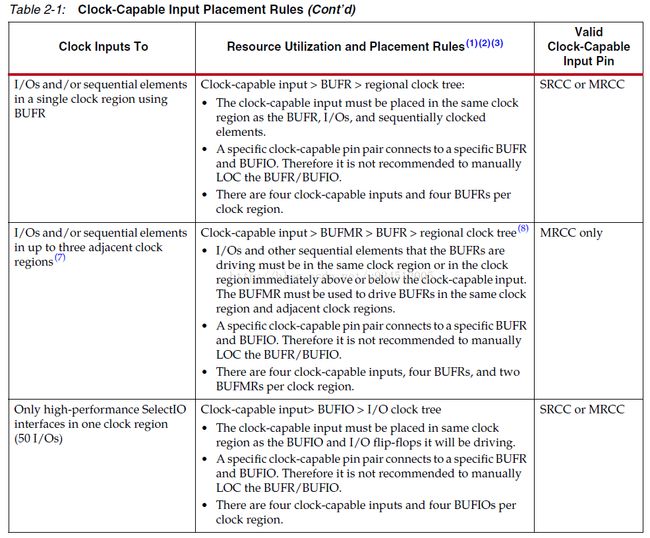
8. SRCC、MRCC:————MRCCs can access multiple clock regions and the global clock tree. MRCCs function the same as SRCCs and can additionally drive multi-clock region buffers (BUFMR) to access up to three clock regions. SRCCs access a single clock region and the global clock tree, as well as other CMTs above and below in the same column.
9. Rules for clock pins:
10. BUFGCTRL、BUFG、BUFGMUX_CTRL、BUFGCE
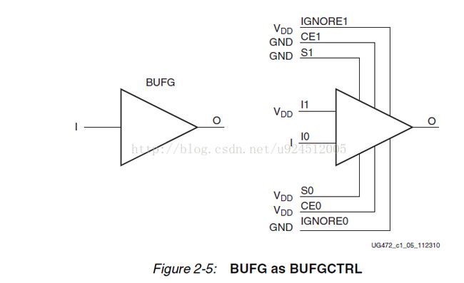
BUFG is a clock buffer with one clock input and one clock output. This primitive is based on BUFGCTRL with some pins connected to logic High or Low.
11. Regional Clocking Resources
the span of a regional clock signal (BUFR) is limited to one clock region, one I/O clock signal drives a single bank
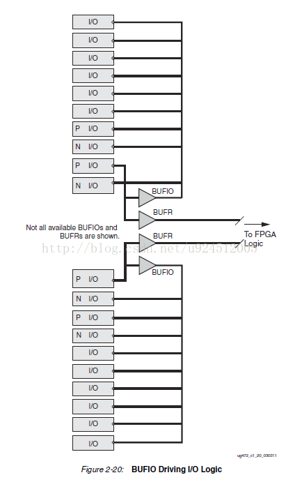
The BUFIO drives a dedicated clock net within the I/O bank, independent of the global clocking resources. Thus, BUFIOs are ideally suited for source-synchronous data capture (forwarded/receiver clock distribution).
BUFRs drive clock signals to a dedicated clock net within a clock region, independent from the global clock tree. Each BUFR can drive the four regional clock nets in the region it is located. Unlike BUFIOs, BUFRs can drive the I/O logic and logic resources (CLB, block RAM, etc.). Clock division in the BUFR is controlled in software through the BUFR_DIVIDE attribute.
BUFRs are ideal for source-synchronous applications requiring clock domain crossing or serial-to-parallel conversion. Unlike BUFIOs, BUFRs are capable of clocking logic resources in the FPGAs other than the IOBs. Figure 2-23 is a BUFR design example.

12. Multi-Region Clock Buffer—BUFMR/BUFMRCE
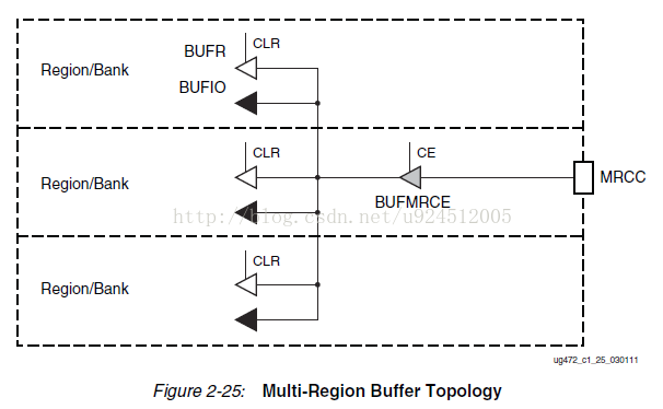
The BUFMR replaces the multi-region/bank support for BUFR and BUFIO available in previous Virtex architectures. There are two BUFMRs in every bank and each buffer can be driven by one specific MRCC in the same bank.
The BUFMRs drive the BUFIOs and/or BUFRs in the same region/banks and in the regions/banks above and below.
BUFMRs must drive BUFRs and BUFIOs to route to the same region/bank and adjacent regions/banks.
13. Horizontal Clock Buffer—BUFH, BUFHCE
BUFHs can be driven by:
• MMCM/PLL outputs in the same region.
• BUFG outputs.
• GT output clocks in the same or horizontal adjacent clock region.
• Local interconnect.
• Clock-capable inputs from either the left or right side I/O banks in the same horizontal adjacent regions/banks.
The power consumption and jitter in a BUFH is lower when compared to a BUFG driving two adjacent regions.
14. Clock management tile(CMT)

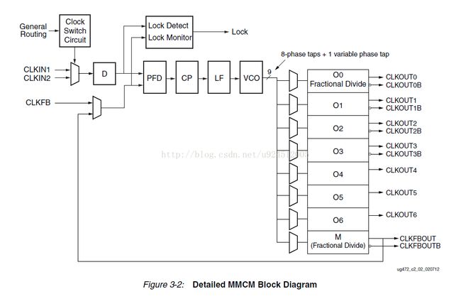

15. MMCM and PLL Use Models
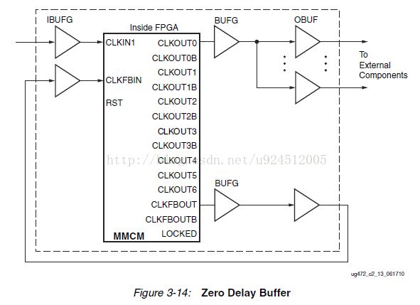
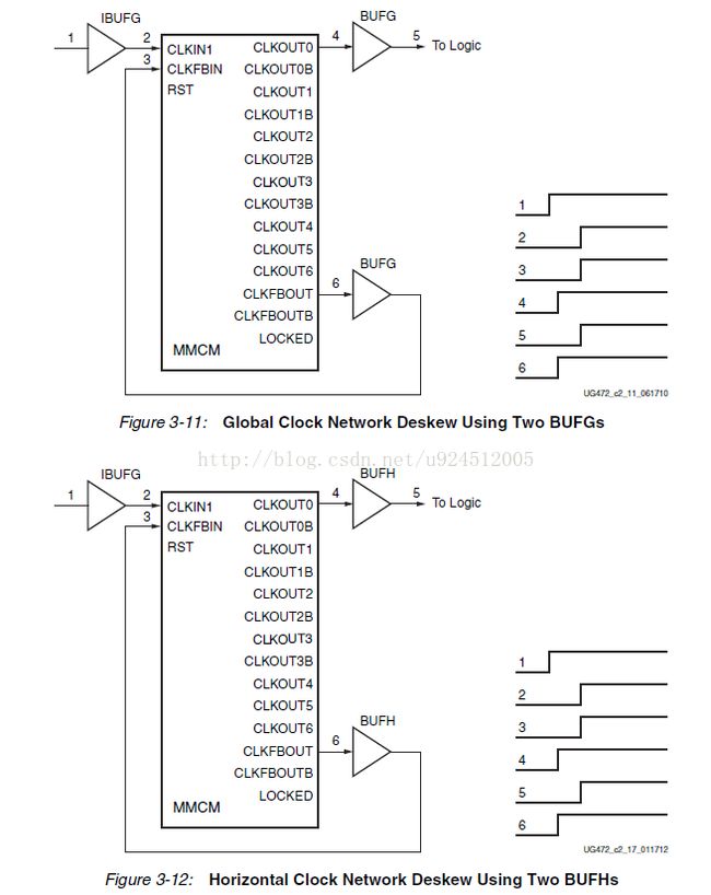
Clock Network DeskewL: The clock output from one of the CLKOUT counters is used to drive logic within the fabric and/or the I/Os. The feedback counter is used to control the exact phase relationship between the input clock and the output clock.
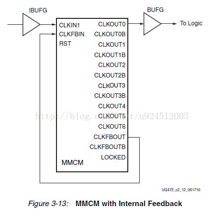
MMCM with Internal Feedback---when the MMCM is used as a synthesizer or jitter filter and there is no required phase relationship between the MMCM input clock and the MMCM output clock.

2. The horizontal clock buffers (BUFH) drive through the HROW to every clocking point in the region. BUFGs and BUFHs share routing tracks in the HROW. The I/O buffers (BUFIO) and regional clock buffers (BUFR) are located inside the I/O banks. The BUFIO only drives I/O clocking resources while the BUFR drives I/O resources and logic resources. The BUFMR enables multi-region chaining of BUFIOs and BUFRs.
BUFG and BUFH share 12 routing tracks in the HROW and can drive all clocking points in the region. BUFGs can also drive BUFHs (not shown in Figure 1-4). This allows for individual clock enables (CE) on an otherwise global clock distribution. A GT quad has ten dedicated tracks to drive the CMT and clock buffers in the clock backbone. The BUFRs located in the I/O bank have four tracks driving clocking points in the logic, CMT, and BUFG. CMTs can, with limitations, drive other CMTs in the adjacent regions using the CMT backbone. Similarly, clock-capable pins can drive, with the same limitations, CMTs in adjacent regions. Clock-capable pins can drive BUFGs anywhere in the same top/bottom side of the device. There are four tracks in the CMT backbone to support connectivity between vertical regions.
Clock sources from one region can drive clock buffer resources in its own region as well as in a horizontally adjacent region. CMTs, clock-capable pins, and serial transceivers can drive clocks into the horizontal adjacent region via the BUFH and also connect to the BUFGs in the same top/bottom side of the device.


Each I/O bank contains four BUFIOs and four BUFRs. Each of these clock buffers can be driven by a specific clock-capable input clock pin pair or can be driven directly by a specific output clock of the MMCM. Two of the clock-capable input pin pairs, called MRCCs, support a multi-region clocking scheme. An MRCC pin pair can drive a specific BUFMR, which in turn can drive BUFIOs and BUFRs in the same and adjacent regions facilitating multi-region/bank interfaces. Similarly, a GT quad can also drive the BUFMRs.

3. The main purpose of the BUFR and BUFIO combination is to support source-synchronous interfaces. When an interface is placed into a single region, the BUFIO clocks the high-speed side of the SelectIOs and the BUFR clocks the deserialized/serialized side at a lower speed into the FPGA logic providing the clock domain transfer function
4. The horizontal clock buffer BUFH (BUFHCE) is strictly a regional resource and cannot span clock regions above or below. Unlike BUFR, BUFH does not have the ability to divide the clock.
5. BUFHs are the preferred clocking resource when an interface or cloud of logic can be localized to one clock region or two horizontally adjacent clock regions.
6. BUFG、BUFH、BUFIO、BUFR
7. Single-ended clock inputs must be assigned to the P (master) side of the clock-capable input pin pair.If a single-ended clock is connected to the P-side of a differential clock pin pair, the N-side cannot be used as another single-ended clock pin—it can only be used as a user I/O.
8. SRCC、MRCC:————MRCCs can access multiple clock regions and the global clock tree. MRCCs function the same as SRCCs and can additionally drive multi-clock region buffers (BUFMR) to access up to three clock regions. SRCCs access a single clock region and the global clock tree, as well as other CMTs above and below in the same column.
9. Rules for clock pins:


10. BUFGCTRL、BUFG、BUFGMUX_CTRL、BUFGCE
BUFG is a clock buffer with one clock input and one clock output. This primitive is based on BUFGCTRL with some pins connected to logic High or Low.

11. Regional Clocking Resources
the span of a regional clock signal (BUFR) is limited to one clock region, one I/O clock signal drives a single bank
The BUFIO drives a dedicated clock net within the I/O bank, independent of the global clocking resources. Thus, BUFIOs are ideally suited for source-synchronous data capture (forwarded/receiver clock distribution).
BUFRs drive clock signals to a dedicated clock net within a clock region, independent from the global clock tree. Each BUFR can drive the four regional clock nets in the region it is located. Unlike BUFIOs, BUFRs can drive the I/O logic and logic resources (CLB, block RAM, etc.). Clock division in the BUFR is controlled in software through the BUFR_DIVIDE attribute.
BUFRs are ideal for source-synchronous applications requiring clock domain crossing or serial-to-parallel conversion. Unlike BUFIOs, BUFRs are capable of clocking logic resources in the FPGAs other than the IOBs. Figure 2-23 is a BUFR design example.


12. Multi-Region Clock Buffer—BUFMR/BUFMRCE
The BUFMR replaces the multi-region/bank support for BUFR and BUFIO available in previous Virtex architectures. There are two BUFMRs in every bank and each buffer can be driven by one specific MRCC in the same bank.
The BUFMRs drive the BUFIOs and/or BUFRs in the same region/banks and in the regions/banks above and below.
BUFMRs must drive BUFRs and BUFIOs to route to the same region/bank and adjacent regions/banks.

13. Horizontal Clock Buffer—BUFH, BUFHCE
BUFHs can be driven by:
• MMCM/PLL outputs in the same region.
• BUFG outputs.
• GT output clocks in the same or horizontal adjacent clock region.
• Local interconnect.
• Clock-capable inputs from either the left or right side I/O banks in the same horizontal adjacent regions/banks.
The power consumption and jitter in a BUFH is lower when compared to a BUFG driving two adjacent regions.

14. Clock management tile(CMT)


15. MMCM and PLL Use Models
Clock Network DeskewL: The clock output from one of the CLKOUT counters is used to drive logic within the fabric and/or the I/Os. The feedback counter is used to control the exact phase relationship between the input clock and the output clock.

MMCM with Internal Feedback---when the MMCM is used as a synthesizer or jitter filter and there is no required phase relationship between the MMCM input clock and the MMCM output clock.

Zero Delay Buffer------A zero delay buffer can be useful for applications where there is a single clock signal fan out to multiple destinations with a low skew between them.
