Topic On ARM Core
1. Introduction
This essay talks something about ARM core, including Cache, Memory Management Unit, Neon. When facing any problem, please refer to the ARM program mannual. The cortex-a series program manual could be downloaded here, while other documents could be found in the ARM community. First, let’s start with a piece of booting code, which telling us what has the ARM core done before system is booted.
1-1 TSIS (the simple initialization sequence)
reset:
    /* Allow the board to save important registers */
    b   save_boot_params
save_boot_params_ret:
    /* * disable interrupts (FIQ and IRQ), also set the cpu to SVC32 mode, * except if in HYP mode already */
    mrs r0, cpsr
    and r1, r0, #0x1f @ mask mode bits
    teq r1, #0x1a @ test for HYP mode
    bicne   r0, r0, #0x1f @ clear all mode bits
    orrne   r0, r0, #0x13 @ set SVC mode
    orr r0, r0, #0xc0 @ disable FIQ and IRQ
    msr cpsr,r0

/* * Setup vector: * (OMAP4 spl TEXT_BASE is not 32 byte aligned. * Continue to use ROM code vector only in OMAP4 spl) */
#if !(defined(CONFIG_OMAP44XX) && defined(CONFIG_SPL_BUILD))
    /* Set V=0 in CP15 SCTLR register - for VBAR to point to vector */
    mrc p15, 0, r0, c1, c0, 0   @ Read CP15 SCTLR Register
    bic r0, #CR_V @ V = 0
    mcr p15, 0, r0, c1, c0, 0   @ Write CP15 SCTLR Register

    /* Set vector address in CP15 VBAR register */
    ldr r0, =_start
    mcr p15, 0, r0, c12, c0, 0  @Set VBAR
#endif

    /* the mask ROM code should have PLL and others stable */
#ifndef CONFIG_SKIP_LOWLEVEL_INIT
    bl  cpu_init_cp15
    bl  cpu_init_crit
#endif

    bl  _main
this piece of codes comes from uboot/arch/arm/cpu/armv7/start.S, uboot source code could be cloned from git://git.denx.de/u-boot.git. When powered on, or reset
b reset
is the first instruction CPU executes. and this function do things followed:
1. set cpu mode
ensure not in HYPERVISOR mode, more info about hypervisor mode. When not in hypervisor mode, change into supervisor mode in which to fiq and irq.
2. set exception vector table
first, unset CV_R
mrc p15, 0, r0, c1, c0, 0   @ Read CP15 SCTLR Register
bic r0, #CR_V @ V = 0
mcr p15, 0, r0, c1, c0, 0   @ Write CP15 SCTLR Register
ldr r0, =_start
mcr p15, 0, r0, c12, c0, 0  @Set VBAR
then the vector table address (_start) will be set to 0x0000_0000 (when CV_R is zero). Any question about p15 operation could be refered to in [2].
3. cpu init and debug
invalidate TLBS, invalidate iCache. still confused with configs, such as ERRDATA (need reference to reference manual about CP15).
4. board specific initialization
bl cpu_init_crit
...
ENTRY(cpu_init_crit)
b lowlevel_init @ go setup, pll, memory
ENDPROC(cpu_init_crit)
just branch into lowlevel_init which is specific to board info.
5. init C runtime environment
bl _mainset up initial C runtime environment and call board_init_f(0)
simple initialization ends
2. CACHE
As Moor’s law still goes on, cpu clock grows dramatically. However, the frequency of the external buses and of memory devices has not scaled to the same extent. Considering the trade-offs(area/performance/money), vendors usually realize leverised memory architecture, showed as follows. Seeing that L1 cache is harvard architecture, while L2 is in von Neumann architecture. Here are some important points.
PoC (Point Of Coherency): the point at which all blocks that can access memory are guaranteed to see the same copy (coherency) of a memory location. Typically, this will be the main external main system memory.
PoU (Point Of Unification): For a core, it is the point at which the instruction and data caches of the core are guaranteed to see the same copy of a memory location. For example, a unified level 2 cache would be the point of a unification system with Harvard level 1 cache and a TLB for caching translation table entries.
For details, refer to the ARM architecture reference manual, ARMv7-A and ARMv7-R edition
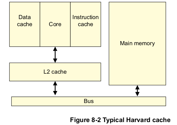
Here are some questions about cache?
1. how the core translates the address to cache-related address?
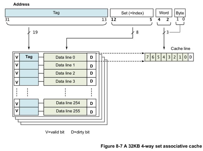
above is a simple example of how the cache controller translates address. When the cache size is 32 Kilo Bytes with 4-way association, we got the cache line number is 32 Kilo Bytes divided by 4 divided by 32, equals 256, with the cache line size 8 words(32 bytes). So we need 8 bits in the address to index the cache line. As we see, bit 5 to bit 12 stands the cache line index. And 3 bits are used to select the word in each line, 2 bits used for selection of bytes in each word. Bits left compose the tag. However there still exists problems. What does the address mean? Is it always the physical address of a word?
2. Cache lookup in detail
As we could see below(Page-117 in arm cortex-a series program manual), different ARM core uses different policies. Here are the two address translation methods. Virtually Indexed, Physically Tagged (VIPT) and Physically Indexed, Virtually Tagged (PIPT). “Early ARM processors such as the ARM720T or ARM926EJ-S processors used virtual addresses to provide both the index and tag values. This has the advantage that the core can do a cache look-up without the need for a virtual to physical address translation. The drawback is that changing the virtual to physical mappings in the system means that the cache must first be cleaned and invalidated, and this can have a significant performance impact.”[1], still confused of “Using a virtual index has some hardware advantages. It means that the cache hardware can read the tag value from the appropriate line in each way in parallel without actually performing the virtual to physical address translation, giving a fast cache response.”
| Processor | |||||
|---|---|---|---|---|---|
| Cortex-A5 | Cortex-A7 | Cortex-A8 | Cortex-A12 | Cortex-A15 | |
| Cache Implementation (data) | PIPT | PIPT | PIPT | PIPT | PIPT |
| Cache Implementation (instruction) | VIPT | VIPT | VIPT | VIPT | VIPT |
| L1 Cache Structure | 2-way set associative (Inst) 4-way set associative (Data) | 2-way set associative (Inst) 4-way set associative (Data) | 4-way set associative | 4-way set associative (Inst) 4-way set associative (Data) | 4-way set associative (Inst) 4-way set associative (Data) |
3. What causes a line from external memory to be placed into the cache? (allocation policy)
4. how the controller decides which line within a set associative cache to use for the incoming data? (replacement policy)
5. What happens when the core performs a write that hits in the cache? (write policy)
A cache lookup on the address(es) to be written is performed, For a cache hit on a write, there are two policies: write through and write back. Write through means when we write to cache, data is also written to the external memory.
6. Do we have any example?
Consider it when you need to copy a piece of code to main memory, such as in boot time. “The memory copy code will use load and store instructions and these will operate on the data side of the core. If the data cache is using a write-back policy for the area to which code is written, it is necessary to clean that data from the cache before the code can be executed. This ensures that the instructions stored as data go out into main memory and are then available for the instruction fetch logic. In addition, if the area to which code is written was previously used for some other program, the instruction cache could contain stale code (from before main memory was re-written). Therefore, it might also be necessary to invalidate the instruction cache before branching to the newly copied code.”
3. MMU
just answer some questions, then we’ll familiar with this block.
1. What does it mean? Memory Management Unit.
It enables you to manage tasks as independent programs running in their own private virtual memory space.
2. Where is it? (architecture)

3. How it works? (function)
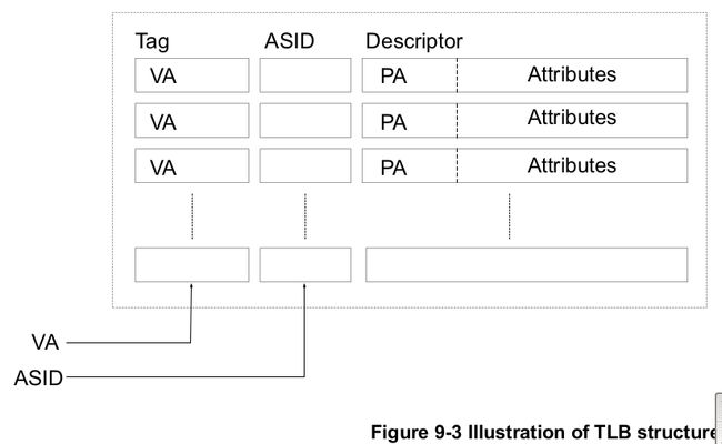
Translation Lookaside Buffer (TLB), the TLB structure is as follows.
A simple example of Translation Table:
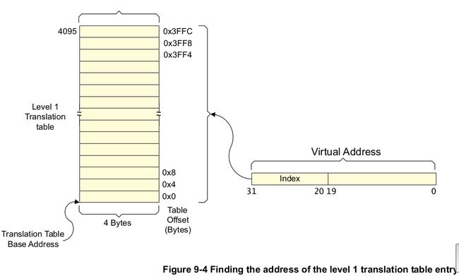
When we got a virtual address, the top 12 bits [31:20] define which 1MB of virtual address space is being accessed. The entry address = Table Base Address + 4 * bits[31:20].

4. How to control/config this module? (program interface)
The TTBR register must be set to point to the tables. The following code sequence can then be used to enable the MMU:
MRC p15, 0, R1, c1, C0, 0   ;Read control register
ORR R1, #0x1    ;Set M bit
MCR p15, 0,R1,C1, C0,0  ;Write control register and enable MMU
Details about p15 operations are in ARM architecture reference manual, ARMv7-A and ARMv7-R edition B3.17
4. NEON
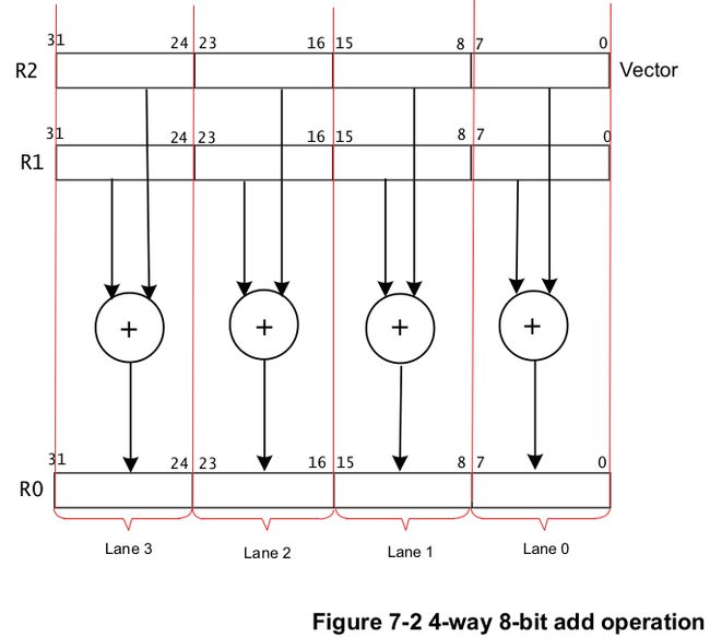
The NEON architecture uses a 32 × 64-bit register file. Since it has individual hardware, instruction set, register file and easily understood by reading the instruction, details are omitted. Examples will be given in the next essays.
5. references
[1] arm cortex-a series program manual
[2] ARM architecture reference manual, ARMv7-A and ARMv7-R edition