HDLBits 系列(14) Latch and Dff and Edge detect
目录
D Latch
DFF + GATE
Mux + DFF
MUX2 + DFF
FSM
JK 触发器
Edgedetect(边沿检测)
双边沿检测
D Latch
Implement the following circuit:
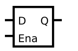
这是一个锁存器,高电平跟随,低电平保持,于是设计:
module top_module (
    input d,
    input ena,
    output q);
    always@(*)begin
        if(ena) q = d;
        else ;
    end

endmodule
DFF + GATE
Implement the following circuit:

module top_module (
    input clk,
    input in,
    output out);
    always@(posedge clk) begin
        out <= in ^ out;
    end

endmodule
Mux + DFF
Taken from ECE253 2015 midterm question 5
Consider the sequential circuit below:
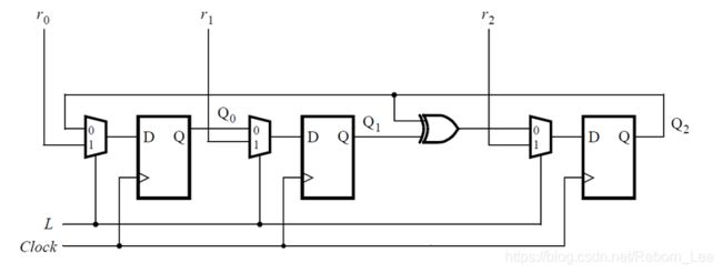
Assume that you want to implement hierarchical Verilog code for this circuit, using three instantiations of a submodule that has a flip-flop and multiplexer in it. Write a Verilog module (containing one flip-flop and multiplexer) named top_module for this submodule.
假设您要使用其中具有触发器和多路复用器的子模块的三个实例化来为此电路实现分层的Verilog代码。 为此子模块编写一个名为top_module的Verilog模块(包含一个触发器和多路复用器)。
要求写出其中一个子模块即可:
module top_module (
	input clk,
	input L,
	input r_in,
	input q_in,
	output reg Q);

	wire mid;
	assign mid = L ? r_in : q_in;

	always@(posedge clk) begin
		Q <= mid;
	end


endmodule
其实读者应该自己用例化的方式,把整个电路实现了。
MUX2 + DFF
Consider the n-bit shift register circuit shown below:
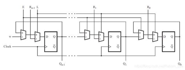
Write a Verilog module named top_module for one stage of this circuit, including both the flip-flop and multiplexers.
module top_module (
    input clk,
    input w, R, E, L,
    output Q
);
	reg Q;
	wire mid1, mid2;
	assign mid1 = E ? w : Q;
	assign mid2 = L ? R : mid1;
	always@(posedge clk) begin
		Q <= mid2;
	end


endmodule
FSM
Given the finite state machine circuit as shown, assume that the D flip-flops are initially reset to zero before the machine begins.
Build this circuit.
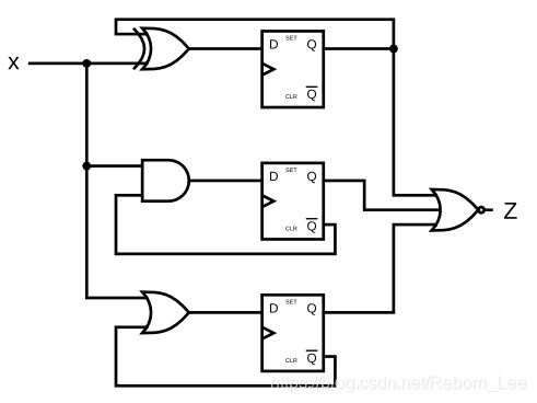
module top_module (
    input clk,
    input x,
    output z
);
reg q1, q2, q3;
always@(posedge clk) begin
	q1 <= q1 ^ x;
	q2 <= ~q2 & x;
	q3 <= ~q3 | x;
end
    assign  z = ~(q1 | q2 | q3);

endmodule
JK 触发器
A JK flip-flop has the below truth table. Implement a JK flip-flop with only a D-type flip-flop and gates. Note: Qold is the output of the D flip-flop before the positive clock edge.
| J | K | Q |
|---|---|---|
| 0 | 0 | Qold |
| 0 | 1 | 0 |
| 1 | 0 | 1 |
| 1 | 1 | ~Qold |
module top_module (
    input clk,
    input j,
    input k,
    output Q);
    always@(posedge clk) begin
        if(~j & ~k) Q <= Q;
        else if(j&k) Q <= ~Q;
        else if(~j & k) Q <= 0;
        else Q <= 1;
    end

endmodule
Edgedetect(边沿检测)
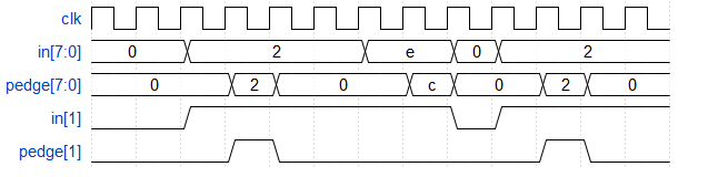
For each bit in an 8-bit vector, detect when the input signal changes from 0 in one clock cycle to 1 the next (similar to positive edge detection). The output bit should be set the cycle after a 0 to 1 transition occurs.
Here are some examples. For clarity, in[1] and pedge[1] are shown separately.
对于8位向量中的每个位,检测输入信号何时从一个时钟周期的0变为下一时钟周期的1(类似于上升沿检测)。 输出位应在发生0到1转换后的周期内进行设置。
这里有些例子。 为了清楚起见,分别显示了in [1]和pedge [1]。
module top_module (
    input clk,
    input [7:0] in,
    output [7:0] pedge
);
    reg [7:0] in_r1, in_r2;
    always@(posedge clk) begin
        in_r1 <= in;
        in_r2 <= in_r1;
    end
    assign pedge = ~in_r2 & in_r1;

endmodule
双边沿检测
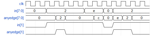
For each bit in an 8-bit vector, detect when the input signal changes from one clock cycle to the next (detect any edge). The output bit should be set the cycle after a 0 to 1 transition occurs.
Here are some examples. For clarity, in[1] and anyedge[1] are shown separately
module top_module (
    input clk,
    input [7:0] in,
    output [7:0] anyedge
);
    reg [7:0] in_r1, in_r2;
    always@(posedge clk) begin
        in_r1 <= in;
        in_r2 <= in_r1;
    end
    assign anyedge = in_r2 ^ in_r1;

endmodule