- HDLBits刷题Day23,3.2.5.7 Simple FSM 3 (asynchronous reset) - 3.2.5.8 Simple FSM 3 (synchronous reset)
weixin_52312830
HDLBits刷题fpga开发算法硬件工程
联系3.2.5.5和3.2.5.6来看3.2.5.7SimpleFSM3(asynchronousreset)问题描述下面是一输入一输出四状态的摩尔状态机的状态转移表。实现这个状态机。包括将FSM重置为状态A的异步重置。代码:moduletop_module(inputclk,inputin,inputareset,outputout);//reg[1:0]state,next_state;par
- HDLBits_Verilog刷题笔记Verilog Language Basics(一)
cascleright1
fpga开发硬件架构
前言这个刷题笔记是给自己复习巩固用的,包括自己在刷题的时候遇到的问题,思考,以及看了一些大佬的笔记和答案进行整理和扩充。git开源solutionshttps://github.com/viduraakalanka/HDL-Bits-Solutionsb站up脱发秘籍搬运工,呜呜这个up不管我学什么都有教程,永远也逃不开脱发的世界~https://space.bilibili.com/318808
- USTC Verilog OJ Solutions
Daniel_187
其他fpga开发VerilogHDLrisc-v
科大OJ其对应的英文版:HDLBits刷题网站01输出1moduletop_module(outputone);assignone=1;endmodule02输出0moduletop_module(outputzero);//Modulebodystartsaftersemicolonassignzero=0;endmodule03wiremoduletop_module(inputin,outp
- FPGA快速入门路径
zuoph
FPGA+人工智能电子技术fpga开发硬件工程
适合新手的FPGA入门路径总体路径规划基础学习-verilog语言verilog语言学习,推荐verilog数字系统设计一书,讲解比较详实和全面。练习推荐使用https://hdlbits.01xz.net/,将所有上面例题自己做一遍,便可做到初步掌握硬件设计语言的使用,想要精通还得自己多看多练,尤其是多练。基础学习-数字电路与系统这方面的书很多,推荐数字设计原理与实践一书,简单的过一遍,以后用到
- 「HDLBits题解」CS450
UESTC_KS
HDLBits题解fpga开发Verilog
本专栏的目的是分享可以通过HDLBits仿真的Verilog代码以提供参考各位可同时参考我的代码和官方题解代码或许会有所收益题目链接:Cs450/timer-HDLBitsmoduletop_module(inputclk,inputload,input[9:0]data,outputtc);reg[9:0]cnt;always@(posedgeclk)beginif(load)cnt<=data
- Verilog刷题[hdlbits] :Bcdadd100
卡布达吃西瓜
verilogfpga开发veriloghdlbits
题目:Bcdadd100YouareprovidedwithaBCDone-digitaddernamedbcd_faddthataddstwoBCDdigitsandcarry-in,andproducesasumandcarry-out.为您提供了一个名为bcd_fadd的BCD一位数加法器,它将两个BCD数字相加并带入,并生成一个和和并带入。modulebcd_fadd(input[3:0]
- Verilog刷题[hdlbits] :Adder100i
卡布达吃西瓜
verilogverilogfpga开发hdlbits
题目:Adder100iCreatea100-bitbinaryripple-carryadderbyinstantiating100fulladders.Theadderaddstwo100-bitnumbersandacarry-intoproducea100-bitsumandcarryout.Toencourageyoutoactuallyinstantiatefulladders,als
- 「HDLBits题解」Verification: Writing Testbenches
UESTC_KS
HDLBits题解fpga开发Verilog
本专栏的目的是分享可以通过HDLBits仿真的Verilog代码以提供参考各位可同时参考我的代码和官方题解代码或许会有所收益题目链接:Tb/clock-HDLBits`timescale1ps/1psmoduletop_module();parametertime_period=10;regclk;initialclk=0;alwaysbegin#(time_period/2)clk=~clk;e
- 「HDLBits题解」Build a circuit from a simulation waveform
UESTC_KS
HDLBits题解fpga开发Verilog
本专栏的目的是分享可以通过HDLBits仿真的Verilog代码以提供参考各位可同时参考我的代码和官方题解代码或许会有所收益题目链接:Sim/circuit1-HDLBitsmoduletop_module(inputa,inputb,outputq);//assignq=a&b;//Fixmeendmodule题目链接:Sim/circuit2-HDLBitsmoduletop_module(i
- 「HDLBits题解」Building Larger Circuits
UESTC_KS
HDLBits题解fpga开发Verilog
本专栏的目的是分享可以通过HDLBits仿真的Verilog代码以提供参考各位可同时参考我的代码和官方题解代码或许会有所收益题目链接:Exams/review2015count1k-HDLBitsmoduletop_module(inputclk,inputreset,output[9:0]q);always@(posedgeclk)beginif(reset)q=0)if(cnt<999)cnt
- 「HDLBits题解」Finite State Machines
UESTC_KS
HDLBits题解fpga开发Verilog
本专栏的目的是分享可以通过HDLBits仿真的Verilog代码以提供参考各位可同时参考我的代码和官方题解代码或许会有所收益题目链接:Fsm1-HDLBitsmoduletop_module(inputclk,inputareset,//AsynchronousresettostateBinputin,outputout);//parameterA=0,B=1;regstate,next_stat
- 【Verilog】HDLBits刷题 03 Verilog语言(2)(未完)
圆喵喵Won
fpga开发
二、模块(module)1.实例化Thefigurebelowshowsaverysimplecircuitwithasub-module.Inthisexercise,createoneinstanceofmodulemod_a,thenconnectthemodule'sthreepins(in1,in2,andout)toyourtop-levelmodule'sthreeports(wir
- 「HDLBits题解」Cellular automata
UESTC_KS
HDLBits题解fpga开发Verilog
本专栏的目的是分享可以通过HDLBits仿真的Verilog代码以提供参考各位可同时参考我的代码和官方题解代码或许会有所收益题目链接:Rule90-HDLBitsmoduletop_module(inputclk,inputload,input[511:0]data,output[511:0]q);always@(posedgeclk)beginif(load)q<=data;elseq<={1'
- 「HDLBits题解」Shift Registers
UESTC_KS
HDLBits题解fpga开发Verilog
本专栏的目的是分享可以通过HDLBits仿真的Verilog代码以提供参考各位可同时参考我的代码和官方题解代码或许会有所收益题目链接:Shift4-HDLBitsmoduletop_module(inputclk,inputareset,//asyncactive-highresettozeroinputload,inputena,input[3:0]data,outputreg[3:0]q);a
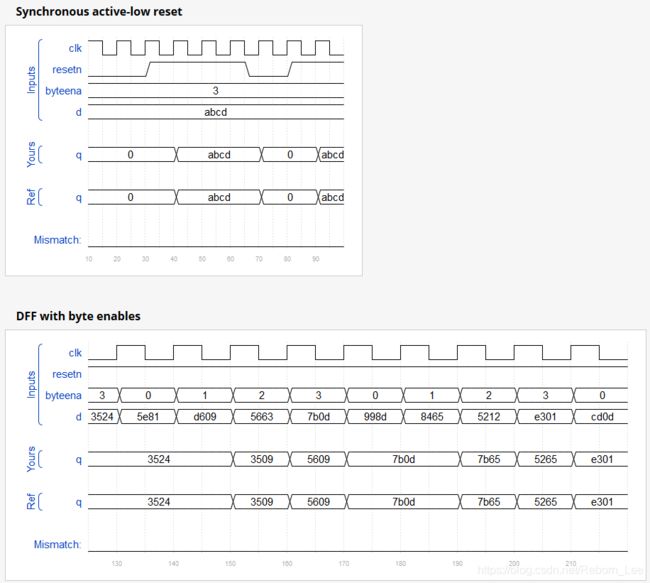
- 「HDLBits题解」Latches and Flip-Flops
UESTC_KS
HDLBits题解fpga开发Verilog
本专栏的目的是分享可以通过HDLBits仿真的Verilog代码以提供参考各位可同时参考我的代码和官方题解代码或许会有所收益题目链接:Dff-HDLBitsmoduletop_module(inputclk,//Clocksareusedinsequentialcircuitsinputd,outputregq);////Useaclockedalwaysblock//copydtoqatever
- 「HDLBits题解」Counters
UESTC_KS
HDLBits题解fpga开发Verilog
本专栏的目的是分享可以通过HDLBits仿真的Verilog代码以提供参考各位可同时参考我的代码和官方题解代码或许会有所收益题目链接:Count15-HDLBitsmoduletop_module(inputclk,inputreset,//Synchronousactive-highresetoutput[3:0]q);always@(posedgeclk)beginif(reset)q<=0;
- verilog语法进阶
FPGA中国创新中心
FPGA学习fpga开发verilogfpga硬件工程
文章目录前言一、always块(alwaysblock)二、if语句三、case语句四、casez语句五、三目运算(ternaryconditionaloperator)六、递减运算符(reduction)七、for循环语句八、实例化多个模块(generate)总结前言 本文是针对verilog基础语法做进一步的学,通过网站HDLbits中的代码和例子来展开本文要讨论的内容。HDLbits是一个
- 「HDLBits题解」Popcount255
UESTC_KS
HDLBits题解Verilog
本专栏的目的是分享可以通过HDLBits仿真的Verilog代码以提供参考各位可同时参考我的代码和官方题解代码或许会有所收益题目链接:Popcount255-HDLBitsmoduletop_module(input[254:0]in,outputreg[7:0]out);integeri;always@(*)beginout=0;for(i=0;i>i&1)out=out+1;elseout=o
- 「HDLBits题解」Adder100i
UESTC_KS
HDLBits题解Verilog
本专栏的目的是分享可以通过HDLBits仿真的Verilog代码以提供参考各位可同时参考我的代码和官方题解代码或许会有所收益题目链接:Adder100i-HDLBitsmoduletop_module(input[99:0]a,b,inputcin,output[99:0]cout,output[99:0]sum);add1Add0(a[0],b[0],cin,sum[0],cout[0]);ge
- 「HDLBits题解」Ringer
UESTC_KS
HDLBits题解Verilog
本专栏的目的是分享可以通过HDLBits仿真的Verilog代码以提供参考各位可同时参考我的代码和官方题解代码或许会有所收益题目链接:Ringer-HDLBitsmoduletop_module(inputring,inputvibrate_mode,outputringer,//Makesoundoutputmotor//Vibrate);assignmotor=vibrate_mode?(ri
- 「HDLBits题解」Bcdadd100
UESTC_KS
HDLBits题解Verilog
本专栏的目的是分享可以通过HDLBits仿真的Verilog代码以提供参考各位可同时参考我的代码和官方题解代码或许会有所收益题目链接:Bcdadd100-HDLBitsmoduletop_module(input[399:0]a,b,inputcin,outputcout,output[399:0]sum);wire[99:0]t;genvari;bcd_faddu0(a[3:0],b[3:0],
- 【Verilog】HDLBits题解——Circuits/Sequential Logic
wjh776a68
#Verilog入门verilogHDLBitsfpga
SequentialLogicLatchesandFlip-FlopsDflip-flop题目链接moduletop_module(inputclk,//Clocksareusedinsequentialcircuitsinputd,outputregq);////Useaclockedalwaysblock//copydtoqateverypositiveedgeofclk//Clockedal
- 【Verilog】HDLBits题解——Verilog Language
wjh776a68
#Verilog入门HDLBitsVerilog题解
BasicsSimplewire题目链接moduletop_module(inputin,outputout);assignout=in;endmoduleFourwires题目链接moduletop_module(inputa,b,c,outputw,x,y,z);assignw=a;assignx=b;assigny=b;assignz=c;endmoduleInverter题目链接modul
- 【Verilog】HDLBits题解——Circuits/Combinational Logic
wjh776a68
#Verilog入门VerilogHDLBits题解
CombinationalLogicBasicGatesWire题目链接moduletop_module(inputin,outputout);assignout=in;endmoduleGND题目链接moduletop_module(outputout);assignout=0;endmoduleNOR题目链接moduletop_module(inputin1,inputin2,outputou
- 【Verilog】HDLBits题解——Verification: Writing Testbenches
wjh776a68
#Verilog入门verilogHDLBitsfpga
Clock题目链接moduletop_module();regclk;initialbeginclk=0;forever#5clk=~clk;enddutdut_inst(.clk(clk));endmoduleTestbench1题目链接moduletop_module(outputregA,outputregB);////generateinputpatternshereinitialbegi
- HDLBits Bcdadd100
yezhangyinge
Verilog题解verilog
该题是根据已经写好的十进制加法器(BCDone-digitadder)module来构建100位十进制加法器BCDone-digitadder如下modulebcd_fadd{input[3:0]a,input[3:0]b,inputcin,outputcout,output[3:0]sum);分析显然可以根据二进制的100位加法器的思路,先进行初始化,但是此时我们无法使用简单的寄存器操作来实现功
- HDLbits Conwaylife题目的一种解法
WaterSplash
fpgaverilog
前言最近在刷HDLBits准备今年的提前批和人秋招,目前刷到有限状态机后,发现前面的大部分题目比较基础。目前比较有难度和有意思的题目就是Conwaylife,二维元胞自动机。这里仅提供笔者自己的解法。解题思路比较好想到的方法就是暴力枚举所有情况,给出该情况下所有的相邻坐标。思考过后觉得暴力枚举容易出现遗漏的情况。有没有一种通用的方法可以处理所有坐标呢。参考生命游戏的前两道题,使用另外两个向量,表示
- 「HDLBits题解」Always casez
UESTC_KS
HDLBits题解fpga开发Verilog
本专栏的目的是分享可以通过HDLBits仿真的Verilog代码以提供参考各位可同时参考我的代码和官方题解代码或许会有所收益题目链接:Alwayscasez-HDLBits//synthesisverilog_input_versionverilog_2001moduletop_module(input[7:0]in,outputreg[2:0]pos);always@(*)begincasez(
- 「HDLBits题解」Always nolatches
UESTC_KS
HDLBits题解Verilog
本专栏的目的是分享可以通过HDLBits仿真的Verilog代码以提供参考各位可同时参考我的代码和官方题解代码或许会有所收益题目链接:Alwaysnolatches-HDLBits//synthesisverilog_input_versionverilog_2001moduletop_module(input[15:0]scancode,outputregleft,outputregdown,o
- 「HDLBits题解」Module cseladd
UESTC_KS
HDLBits题解fpga开发Verilog
本专栏的目的是分享可以通过HDLBits仿真的Verilog代码以提供参考各位可同时参考我的代码和官方题解代码或许会有所收益题目链接:Modulecseladd-HDLBitsmoduletop_module(input[31:0]a,input[31:0]b,output[31:0]sum);wirecout1,cout2,cout3;wire[15:0]t1,t2,t3,t4;reg[15:0
- windows下源码安装golang
616050468
golang安装golang环境windows
系统: 64位win7, 开发环境:sublime text 2, go版本: 1.4.1
1. 安装前准备(gcc, gdb, git)
golang在64位系
- redis批量删除带空格的key
bylijinnan
redis
redis批量删除的通常做法:
redis-cli keys "blacklist*" | xargs redis-cli del
上面的命令在key的前后没有空格时是可以的,但有空格就不行了:
$redis-cli keys "blacklist*"
1) "blacklist:12:
[email protected]
- oracle正则表达式的用法
0624chenhong
oracle正则表达式
方括号表达示
方括号表达式
描述
[[:alnum:]]
字母和数字混合的字符
[[:alpha:]]
字母字符
[[:cntrl:]]
控制字符
[[:digit:]]
数字字符
[[:graph:]]
图像字符
[[:lower:]]
小写字母字符
[[:print:]]
打印字符
[[:punct:]]
标点符号字符
[[:space:]]
- 2048源码(核心算法有,缺少几个anctionbar,以后补上)
不懂事的小屁孩
2048
2048游戏基本上有四部分组成,
1:主activity,包含游戏块的16个方格,上面统计分数的模块
2:底下的gridview,监听上下左右的滑动,进行事件处理,
3:每一个卡片,里面的内容很简单,只有一个text,记录显示的数字
4:Actionbar,是游戏用重新开始,设置等功能(这个在底下可以下载的代码里面还没有实现)
写代码的流程
1:设计游戏的布局,基本是两块,上面是分
- jquery内部链式调用机理
换个号韩国红果果
JavaScriptjquery
只需要在调用该对象合适(比如下列的setStyles)的方法后让该方法返回该对象(通过this 因为一旦一个函数称为一个对象方法的话那么在这个方法内部this(结合下面的setStyles)指向这个对象)
function create(type){
var element=document.createElement(type);
//this=element;
- 你订酒店时的每一次点击 背后都是NoSQL和云计算
蓝儿唯美
NoSQL
全球最大的在线旅游公司Expedia旗下的酒店预订公司,它运营着89个网站,跨越68个国家,三年前开始实验公有云,以求让客户在预订网站上查询假期酒店时得到更快的信息获取体验。
云端本身是用于驱动网站的部分小功能的,如搜索框的自动推荐功能,还能保证处理Hotels.com服务的季节性需求高峰整体储能。
Hotels.com的首席技术官Thierry Bedos上个月在伦敦参加“2015 Clou
- java笔记1
a-john
java
1,面向对象程序设计(Object-oriented Propramming,OOP):java就是一种面向对象程序设计。
2,对象:我们将问题空间中的元素及其在解空间中的表示称为“对象”。简单来说,对象是某个类型的实例。比如狗是一个类型,哈士奇可以是狗的一个实例,也就是对象。
3,面向对象程序设计方式的特性:
3.1 万物皆为对象。
- C语言 sizeof和strlen之间的那些事 C/C++软件开发求职面试题 必备考点(一)
aijuans
C/C++求职面试必备考点
找工作在即,以后决定每天至少写一个知识点,主要是记录,逼迫自己动手、总结加深印象。当然如果能有一言半语让他人收益,后学幸运之至也。如有错误,还希望大家帮忙指出来。感激不尽。
后学保证每个写出来的结果都是自己在电脑上亲自跑过的,咱人笨,以前学的也半吊子。很多时候只能靠运行出来的结果再反过来
- 程序员写代码时就不要管需求了吗?
asia007
程序员不能一味跟需求走
编程也有2年了,刚开始不懂的什么都跟需求走,需求是怎样就用代码实现就行,也不管这个需求是否合理,是否为较好的用户体验。当然刚开始编程都会这样,但是如果有了2年以上的工作经验的程序员只知道一味写代码,而不在写的过程中思考一下这个需求是否合理,那么,我想这个程序员就只能一辈写敲敲代码了。
我的技术不是很好,但是就不代
- Activity的四种启动模式
百合不是茶
android栈模式启动Activity的标准模式启动栈顶模式启动单例模式启动
android界面的操作就是很多个activity之间的切换,启动模式决定启动的activity的生命周期 ;
启动模式xml中配置
<activity android:name=".MainActivity" android:launchMode="standard&quo
- Spring中@Autowired标签与@Resource标签的区别
bijian1013
javaspring@Resource@Autowired@Qualifier
Spring不但支持自己定义的@Autowired注解,还支持由JSR-250规范定义的几个注解,如:@Resource、 @PostConstruct及@PreDestroy。
1. @Autowired @Autowired是Spring 提供的,需导入 Package:org.springframewo
- Changes Between SOAP 1.1 and SOAP 1.2
sunjing
ChangesEnableSOAP 1.1SOAP 1.2
JAX-WS
SOAP Version 1.2 Part 0: Primer (Second Edition)
SOAP Version 1.2 Part 1: Messaging Framework (Second Edition)
SOAP Version 1.2 Part 2: Adjuncts (Second Edition)
Which style of WSDL
- 【Hadoop二】Hadoop常用命令
bit1129
hadoop
以Hadoop运行Hadoop自带的wordcount为例,
hadoop脚本位于/home/hadoop/hadoop-2.5.2/bin/hadoop,需要说明的是,这些命令的使用必须在Hadoop已经运行的情况下才能执行
Hadoop HDFS相关命令
hadoop fs -ls
列出HDFS文件系统的第一级文件和第一级
- java异常处理(初级)
白糖_
javaDAOspring虚拟机Ajax
从学习到现在从事java开发一年多了,个人觉得对java只了解皮毛,很多东西都是用到再去慢慢学习,编程真的是一项艺术,要完成一段好的代码,需要懂得很多。
最近项目经理让我负责一个组件开发,框架都由自己搭建,最让我头疼的是异常处理,我看了一些网上的源码,发现他们对异常的处理不是很重视,研究了很久都没有找到很好的解决方案。后来有幸看到一个200W美元的项目部分源码,通过他们对异常处理的解决方案,我终
- 记录整理-工作问题
braveCS
工作
1)那位同学还是CSV文件默认Excel打开看不到全部结果。以为是没写进去。同学甲说文件应该不分大小。后来log一下原来是有写进去。只是Excel有行数限制。那位同学进步好快啊。
2)今天同学说写文件的时候提示jvm的内存溢出。我马上反应说那就改一下jvm的内存大小。同学说改用分批处理了。果然想问题还是有局限性。改jvm内存大小只能暂时地解决问题,以后要是写更大的文件还是得改内存。想问题要长远啊
- org.apache.tools.zip实现文件的压缩和解压,支持中文
bylijinnan
apache
刚开始用java.util.Zip,发现不支持中文(网上有修改的方法,但比较麻烦)
后改用org.apache.tools.zip
org.apache.tools.zip的使用网上有更简单的例子
下面的程序根据实际需求,实现了压缩指定目录下指定文件的方法
import java.io.BufferedReader;
import java.io.BufferedWrit
- 读书笔记-4
chengxuyuancsdn
读书笔记
1、JSTL 核心标签库标签
2、避免SQL注入
3、字符串逆转方法
4、字符串比较compareTo
5、字符串替换replace
6、分拆字符串
1、JSTL 核心标签库标签共有13个,
学习资料:http://www.cnblogs.com/lihuiyy/archive/2012/02/24/2366806.html
功能上分为4类:
(1)表达式控制标签:out
- [物理与电子]半导体教材的一个小问题
comsci
问题
各种模拟电子和数字电子教材中都有这个词汇-空穴
书中对这个词汇的解释是; 当电子脱离共价键的束缚成为自由电子之后,共价键中就留下一个空位,这个空位叫做空穴
我现在回过头翻大学时候的教材,觉得这个
- Flashback Database --闪回数据库
daizj
oracle闪回数据库
Flashback 技术是以Undo segment中的内容为基础的, 因此受限于UNDO_RETENTON参数。要使用flashback 的特性,必须启用自动撤销管理表空间。
在Oracle 10g中, Flash back家族分为以下成员: Flashback Database, Flashback Drop,Flashback Query(分Flashback Query,Flashbac
- 简单排序:插入排序
dieslrae
插入排序
public void insertSort(int[] array){
int temp;
for(int i=1;i<array.length;i++){
temp = array[i];
for(int k=i-1;k>=0;k--)
- C语言学习六指针小示例、一维数组名含义,定义一个函数输出数组的内容
dcj3sjt126com
c
# include <stdio.h>
int main(void)
{
int * p; //等价于 int *p 也等价于 int* p;
int i = 5;
char ch = 'A';
//p = 5; //error
//p = &ch; //error
//p = ch; //error
p = &i; //
- centos下php redis扩展的安装配置3种方法
dcj3sjt126com
redis
方法一
1.下载php redis扩展包 代码如下 复制代码
#wget http://redis.googlecode.com/files/redis-2.4.4.tar.gz
2 tar -zxvf 解压压缩包,cd /扩展包 (进入扩展包然后 运行phpize 一下是我环境中phpize的目录,/usr/local/php/bin/phpize (一定要
- 线程池(Executors)
shuizhaosi888
线程池
在java类库中,任务执行的主要抽象不是Thread,而是Executor,将任务的提交过程和执行过程解耦
public interface Executor {
void execute(Runnable command);
}
public class RunMain implements Executor{
@Override
pub
- openstack 快速安装笔记
haoningabc
openstack
前提是要配置好yum源
版本icehouse,操作系统redhat6.5
最简化安装,不要cinder和swift
三个节点
172 control节点keystone glance horizon
173 compute节点nova
173 network节点neutron
control
/etc/sysctl.conf
net.ipv4.ip_forward =
- 从c面向对象的实现理解c++的对象(二)
jimmee
C++面向对象虚函数
1. 类就可以看作一个struct,类的方法,可以理解为通过函数指针的方式实现的,类对象分配内存时,只分配成员变量的,函数指针并不需要分配额外的内存保存地址。
2. c++中类的构造函数,就是进行内存分配(malloc),调用构造函数
3. c++中类的析构函数,就时回收内存(free)
4. c++是基于栈和全局数据分配内存的,如果是一个方法内创建的对象,就直接在栈上分配内存了。
专门在
- 如何让那个一个div可以拖动
lingfeng520240
html
<!DOCTYPE html PUBLIC "-//W3C//DTD XHTML 1.0 Transitional//EN" "http://www.w3.org/TR/xhtml1/DTD/xhtml1-transitional.dtd">
<html xmlns="http://www.w3.org/1999/xhtml
- 第10章 高级事件(中)
onestopweb
事件
index.html
<!DOCTYPE html PUBLIC "-//W3C//DTD XHTML 1.0 Transitional//EN" "http://www.w3.org/TR/xhtml1/DTD/xhtml1-transitional.dtd">
<html xmlns="http://www.w3.org/
- 计算两个经纬度之间的距离
roadrunners
计算纬度LBS经度距离
要解决这个问题的时候,到网上查了很多方案,最后计算出来的都与百度计算出来的有出入。下面这个公式计算出来的距离和百度计算出来的距离是一致的。
/**
*
* @param longitudeA
* 经度A点
* @param latitudeA
* 纬度A点
* @param longitudeB
*
- 最具争议的10个Java话题
tomcat_oracle
java
1、Java8已经到来。什么!? Java8 支持lambda。哇哦,RIP Scala! 随着Java8 的发布,出现很多关于新发布的Java8是否有潜力干掉Scala的争论,最终的结论是远远没有那么简单。Java8可能已经在Scala的lambda的包围中突围,但Java并非是函数式编程王位的真正觊觎者。
2、Java 9 即将到来
Oracle早在8月份就发布
- zoj 3826 Hierarchical Notation(模拟)
阿尔萨斯
rar
题目链接:zoj 3826 Hierarchical Notation
题目大意:给定一些结构体,结构体有value值和key值,Q次询问,输出每个key值对应的value值。
解题思路:思路很简单,写个类词法的递归函数,每次将key值映射成一个hash值,用map映射每个key的value起始终止位置,预处理完了查询就很简单了。 这题是最后10分钟出的,因为没有考虑value为{}的情